Standard Cell Library Design And Characterization Using .
IOSR Journal of VLSI and Signal Processing (IOSR-JVSP)Volume 4, Issue 1, Ver. I (Jan. 2014), PP 29-33e-ISSN: 2319 – 4200, p-ISSN No. : 2319 – 4197www.iosrjournals.orgStandard Cell Library Design and Characterization using 45nmtechnology1Prof. Poornima H S, 2Prof. Chethana K S,1Dept of ECE, VVCE, Mysore, IndiaDept of ECE, VVCE, Mysore, India2Abstract: Producing designs based on sub-micron technologies at a competitive cost has always been achallenge for the manufacturers. Different Integrated Circuit (IC) implementation approaches have beenadopted to reduce the design time and improve manufacturing costs. One of the methods is to use a ‘Cell-Based’IC implementation approach using Standard Cell Libraries However, the cost associated with the design orpurchase of Standard Cell Libraries (Non-Recurring Expense (NRE)) has been increasing consistently with theshortening of device technology. In this paper we present the development of submicron CMOS Standard CellLibrary that is suitable for 45nm CMOS process The intent was to generate a comprehensive library containingcore number of necessary cells, providing detailed layout and transistor-level schematic views of every cell,with characterization under the 45nm process, in order to utilize them as a fully synthesizable library. Thelibrary is designed using Cadence.Index Terms: standard cell library, 45nm process, layout design, characterizationI.IntroductionIntegrated Circuit (IC) technology has gone through a spectacular revolution in the last two decades.The number of transistors that can be integrated on a single die has been exponentially increasing with timefollowing the Moore‟s Law. Present day microprocessors have more than one million transistors and are clockedat Giga Hertz (GHz) clock speeds. Bringing these high development cost associated high performance designsto the market at a competitive cost and in a lesser design time has always been a challenge for IC manufactures.To meet these challenges, different IC implementation approaches have been adopted ranging from customdesign approach, used for microprocessors and memories to the fully programmable designs for medium – to –low performance applicationsA.Cell Based Semi-Custom DesignWith the advancement of design automation, Cell Based Semi-Custom IC implementation approacheshave been introduced to shorten and automate the design process. The idea behind „Cell Based‟ design is toreduce the design cost and design time by reusing a library of cells called Standard Cell Library. Thedisadvantage is that the cells in the library decide the integration density and/or performance reducing the abilityto fine-tune the IC design.B.Standard Cell LibraryThe Standard Cell Library contains a collection of logic gates over a range of fan-in and fan-out.Besides the basic logic function, such as inverter, NAND, NOR, XOR and Flip- Flops, a typical library alsocontains more complex functions such as Multiplexers, Full-Adder, Comparator, etc. As shown in Fig 1, theStandard Cell Library is used in the Semi-Custom Design Flow to shorten the design process.Fig 1: Semi–Custom Design Flowwww.iosrjournals.org29 Page
Standard Cell Library Design and Characterization using 45nm technologyIt should be noted that a successful and efficient implementation of a Semi-Custom Design depends onthe standard cells in the library. Therefore, it is important to have a „high quality cell library‟.A „high quality cell library‟ possesses many common characteristics including: Cells functionality being correct. Cells timing performance claimed in the data sheet being accurate enough. Cells having no design rule violations in their layouts. Cells can be utilized in the best way using a synthesizer. Cells can optimize placement and route of a large design.These characteristics help in an efficient integration of Standard Cell Library into a Semi- Custom Design Flow.A typical standard-cell library contains two main components:1.Library Database - Consists of a number of views often including layout, schematic, symbol, abstract,and other logical or simulation views. From this, various information may be captured in a number of formatsincluding the Cadence LEF format, and the Synopsys Milky way format, which contain reduced informationabout the cell layouts, sufficient for automated "Place and Route" tools.2.Timing Abstract - Generally in Liberty format, to provide functional definitions, timing, power, andnoise information for each cell.A standard-cell library may also contain the following additional components: A full layout of the cells Spice models of the cells Verilog models or VHDL Vital models Parasitic Extraction models DRC rule checksII.Standard Cell Library DesignThe „Cells‟ or logic gates selected to build the library depends on the design requirement. These cellswhen used in the Semi-Custom Design Flow have to meet certain functions and performance. The cells areeither area optimized or speed optimized. The area optimized cells uses minimum sized transistors while thespeed optimized cells uses larger transistors to provide good driving capabilities. The Standard Cell Librarydevelopment process can be depicted using a flow chart as shown in Fig 2.The design specification of a particular cell in the library is decided and the initial design is done. It ischecked whether the design meets the required specification. After this, the „Layout‟ of the designed cell iscarried out and a netlist is extracted from the „Layout‟. The netlist obtained from the „Layout‟ is compared withthe initial design. If the results match, then the design cycle is complete else, redesigning has to be carried outand the cycle is repeated.The sizes of PMOS (Wp) and NMOS (Wn) of the transistors in the Cells are selected to meet designspecifications such as power dissipation, delay, noise immunity and area. Therefore, the sizing constraint forStandard Library Cells is similar to any MOS circuit design requirement of minimum area subject to delay lessthan or equal to the required timing specification. Therefore, Wp and Wn are determined by DC switching point. Drive capability of the cell.It should be noted that while designing the cells and deciding the „sizes‟ of the cells, process variationsshould also be considered for proper functioning cells at the end of fabrication. After the cells have beendesigned and simulated, to ensure proper functionality and timing, cells have to be characterized to obtaindifferent parameters (power, timing, etc.). This requires multiple executions of circuit simulators for each cell.An „automatic cell characterization tools‟ are used for this purpose. The final requirement is documentation thatsummarizes the functionality and timing of each cell.III.Design Flow Adopted For The Standard Cell Library DevelopmentEach cell in the library was developed using the Bottom-Up design flow. The Bottom-Up Design flowis given in Fig 2. Each block in the figure can be described as follows.A.Design SpecificationsThe Bottom-Up design flow starts with a set of design specifications. The “specs” typically describe theexpected functionality of the designed circuit as well as other properties like delay times, area, etc. To meet thevarious design specifications certain design trade offs (area verses delay) are required.www.iosrjournals.org30 Page
Standard Cell Library Design and Characterization using 45nm technologyB.Schematic CaptureA Schematic Editor is used for capturing (i.e. describing) the transistor-level design. The SchematicEditors provide simple, intuitive means to draw, to place and to connect individual components that make up thedesign. The resulting schematic drawing must accurately describe the main electrical properties of allcomponents and their interconnections. Also included in the schematic are the supply connections (Vdd andGnd), as well as all pins for the input and output signals of the circuit. From the schematic, a netlist is generated,which is used in later stages of the design. The generation of a complete circuit schematic is therefore the firstimportant step of the transistor-level design.Fig 2 design flow of standard cell librarySymbol CreationA symbol view of the circuit is also required for some of the subsequent simulation steps or fordocumentation purposes. Thus, the schematic capture of the circuit topology is usually followed by the creationof a symbol to represent the entire circuit. The shape of the icon to be used for the symbol may suggest thefunction of the module (logic gates – AND, OR, etc.), but the default symbol icon is a simple rectangular boxwith input and output pins. The symbol creation will also help the circuit designer to create a system leveldesign consisting of multiple hierarchy level.C.Table 1: switching characteristics of 2 input XOR gate of different drive strengthsXor2 1xXor2 2xXor2 4xXor2 Tf(ps)25.33422.90222.77623.504CL (LoadCapacitance)Cinv2 Cinv4 Cinv8 CinvD.Pre-Layout simulationAfter the transistor level description of a circuit is completed using the schematic editor, the electricalperformance and the functionality of the circuit must be verified using a simulation tool. Based on simulationresults, the designer usually modifies some of the device properties in order to optimize the performance. Theinitial simulation phase also serves to detect some of the design errors that may have been created during theschematic entry step. Table 1 shows the switching characteristics of 2 input xor gate of different drive strengthsfor pulse input (Ton Toff 10ns, Tr Tf 50ps, Cinv 0.3fF)E.LayoutThe creation of the mask layout is one of the most important steps in the full-custom design flow,where the designer describes the detailed geometrics and the relative positioning of each mask layer to be usedin actual fabrication, using a Layout Editor. Physical layout design is very tightly linked to overall circuitperformance since the physical structures determines the transconductances of the transistors, the parasiticcapacitances and resistances, and obviously the silicon area which is used to realize a certain function. But theprocess is very intensive and time-consuming design effort. It is also extremely important that the layout designwww.iosrjournals.org31 Page
Standard Cell Library Design and Characterization using 45nm technologymust not violate any of the layout design rules, in order to ensure a defect free fabrication of the design. Fig 3shows the layout of 3 input XOR gate of 4x drive strength.The layout process can be a manual process, in which layout of each design is done manually or anautomatic process using a CAD tool. But the quality of the layouts produced using automatic processes are stillfar from hand optimized layouts.F.Design Rule Check (DRC)The created mask layout must conform to a complex set of design rules, in order to ensure a lowerprobability of fabrication defects. A tool built in to the layout editor called Design Rule Checker, is used todetect any design rule violations during and after the mask layout design. If errors are detected, they should beremoved from the mask layout, before the final design is saved.G.Circuit ExtractionAfter the mask layout has been made free from design rule errors, circuit extraction is performed tocreate a detailed netlist for the simulation of the circuit. The circuit extractor identifies the individual transistorsand their connections as well as the parasitic capacitances and resistances that are inevitably present. Theextracted netlist can give a very accurate estimation of the device dimensions and device parasitics thatultimately determine the circuit performance. The extracted netlist are used in transistor level simulations and inLayout Verses Schematic comparison.H. Layout VS Schematic CheckAfter the mask layout design of the circuit is completed, the design should be checked against theschematic circuit description created earlier. The „Layout Verses Schematic (LVS) Check‟ will compare theoriginal network with the one extracted from the mask layout. The LVS step provides an additional level ofconfidence for the integrity of the design, and ensures that the mask layout is a correct realization of theintended circuit topology. Also it should be noted that a successful LVS would not guarantee that the extractedcircuit would actually satisfy the performance requirements since LVS check guarantees only a topologicalmatch. If any errors show up during LVS, then it should be corrected before proceeding to post layoutsimulation.I.Post-Layout SimulationThe electrical performance of a full custom design can be best analyzed by performing a post-layoutsimulation on the extracted circuit netlist. The detailed simulation performed using the extracted netlist willprovide a clear assessment of the circuit speed and the influence of circuit parasitics. If the results of the postlayout simulation are not satisfactory, the designer should modify the transistor dimensions or the circuittopology, in order to achieve the desired circuit performance. Thus, it may require multiple iterations on thedesign, until the postlayout simulation results satisfy the original design requirements. Finally, it should benoted that a satisfactory result in post-layout simulation is still no guarantee for a completely successful product,since the actual performance of the chip can be only be verified by testing the fabricated prototype.Fig: 3 input XOR gate of drive strength 4XIV.Characterization ProcessThe cells are simulated to ensure proper functionality and timing. The results from the initial designand extracted values are compared. There are many models which we can use to simulate the nominal processfrom the fabrication. Measurements of all delay times are at 50% to 50% Vdd values. All rise/fall times are 10%to 90% Vdd values. To obtain realistic manufacturing process characteristic, circuit simulation is performedwith temperature, voltage and process parameter over the range of values that are expected to occur. The criticalvalues at process comer are simulated with minimum and maximum condition. To exercise all input-to-outputwww.iosrjournals.org32 Page
Standard Cell Library Design and Characterization using 45nm technologypaths through the cells, input stimulus will be provided to the circuit simulator. Since many repetitive executionsof the circuit simulator are required for each cell, the characterization is done using an automatic cellcharacterization tool. Table 2 shows characterization values of inverter for process TT, voltage 1.1v andtemperature -40 degree centigrade.Table 2: characterization table of inverterCL (Ff)SLEW(ps)TplhTphlTf5TrC1 0.3C2 0.6C3 515.59412.85823.08130.377After characterizing, the cells functional description and timing data are transformed to the formatrequired by a specific design tools. Most design tools utilize special-purpose model formats with syntax forexplicitly describing propagation delays, timing checks, and other aspects of cell behavior that are required bythe tool. The final requirement is a documentation that summaries the functionality and timing of each cell. Thefunctionality is frequently described with truth table, and timing data is presented in a simple format in thedatasheet. The documentation for each library contains: Setup and hold times Operating range of temperature and voltage Fan-in and fan-out Variation of timing due to temperature and Voltage Path delays Library cell symbol Timing diagrams.V.Conclusion And Future WorksDigital standard cell library is very useful in ASIC design. Standard library cells improve designer‟sproductivity through reduced design time and debugging. Implementing this flow using CAD tools available inmarket, you can design standard cell library.In future more investigations have to be done on the behavior of transistors in series. To improve theefficiency of the library for building complex design, mega cells such as: 1 bit register file slice, a 1 bit ALU, pdecoder, UART, PIO/PIA microcontroller core, fixed point DSP core, FIFO, SRAM should be included in theexisting library. To achieve higher speed and lesser area transistors can be scaled and single and double heightcells can be implemented. Few analog cells and filler cells can be included.AcknowledgementWe pay our due regards to our renowned institution Vidyavardhaka College of Engineering, Mysorewhich provided us a platform and an opportunity for carrying out this [12]Jan M. Rabaey et al., “Digital integrated circuit – A Design Perspective”, Second Edition, Prentice Hall, 2003.HSPICE Reference Manual: Commands and Control Options Version B-2008.09, September 2008 (Synopsis)Ashral bin Bahari Tambek, Ahmad Raif bin Mohd Noor Beg, Mohd Rais Ahmad, “Standard Cell Library development”, inProceedings of the 11th International Conference on Microelectronics, 1999, pp.22-24.Weitong Chuang, Sachin S. Sapatnekar, Ibrahim N. Haji, “Timing and area optimization for Standard-Cell VLSI circuit design”,IEEE Trans. on Computer-Aided Design of Integrated Circuits and Systems, vol. 14, March 1995.CMOS IC LAYOUT Concepts, Methodologies, and Tools by Dan CleinRon Wilson, EE Times, May 2000.www.InnovationRevolution.comMicroelectronics Group at Worchester Polytechnic Institute, “Cadence Design Tools Tutorial”, October kazu Shoji, “CMOS Digital Circuit Technology”, Prentice Hall, 1988.CMOS VLSI Design: A Circuits and Systems Perspective by Neil H.E. Weste, David Harris, Ayan Banerjee, Wesley, 1993.R. Jacob Baker et al., “CMOS – Circuit Design, Layout and Simulation”, Wiley-IEEE Press, 1997.www.mosis.orgwww.iosrjournals.org33 Page
Standard Cell Library Design and Characterization using 45nm technology 1Prof. Poornima H S, 2Prof. Chethana K S, 1Dept of ECE, VVCE, Mysore, India 2Dept of ECE, VVCE, Mysore, India Abstract: Producing designs based on sub-micron technologies at a competitiv
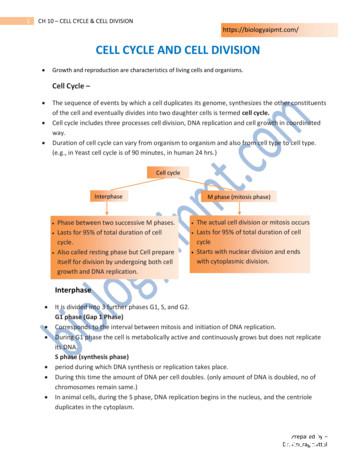
of the cell and eventually divides into two daughter cells is termed cell cycle. Cell cycle includes three processes cell division, DNA replication and cell growth in coordinated way. Duration of cell cycle can vary from organism to organism and also from cell type to cell type. (e.g., in Yeast cell cycle is of 90 minutes, in human 24 hrs.)
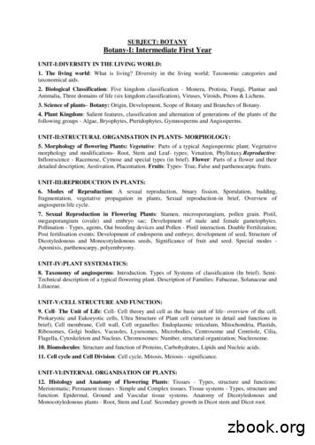
UNIT-V:CELL STRUCTURE AND FUNCTION: 9. Cell- The Unit of Life: Cell- Cell theory and cell as the basic unit of life- overview of the cell. Prokaryotic and Eukoryotic cells, Ultra Structure of Plant cell (structure in detail and functions in brief), Cell membrane, Cell wall, Cell organelles: Endoplasmic reticulum, Mitochondria, Plastids,
Stent Type Stent Design Free Cell Area (mm2) Wallstent Closed cell 1.08 Xact Closed cell 2.74 Neuroguard Closed cell 3.5 Nexstent Closed cell 4.7 Precise Open cell 5.89 Protégé Open cell 20.71 Acculink Open cell 11.48 Stent Free Cell Area Neuroguard IEP Carotid Stent
Stent Type Stent Design Free Cell Area (mm2) Wallstent Closed cell 1.08 Xact Closed cell 2.74 Neuroguard Closed cell 3.5 Nexstent Closed cell 4.7 Precise Open cell 5.89 Protégé Open cell 20.71 Acculink Open cell 11.48 Neuroguard IEP Carotid Stent Stent Free Cell Area
The Cell Cycle The cell cycle is the series of events in the growth and division of a cell. In the prokaryotic cell cycle, the cell grows, duplicates its DNA, and divides by pinching in the cell membrane. The eukaryotic cell cycle has four stages (the first three of which are referred to as interphase): In the G 1 phase, the cell grows.
Many scientists contributed to the cell theory. The cell theory grew out of the work of many scientists and improvements in the . CELL STRUCTURE AND FUNCTION CHART PLANT CELL ANIMAL CELL . 1. Cell Wall . Quiz of the cell Know all organelles found in a prokaryotic cell
Class-XI-Biology Cell Cycle and Cell Division 1 Practice more on Cell Cycle and Cell Division www.embibe.com CBSE NCERT Solutions for Class 11 Biology Chapter 10 Back of Chapter Questions 1. What is the average cell cycle span for a mammalian cell? Solution: The average cell cycle span o
2 - the library building is a public library recognized by the state library agency as a public library; 3 - the library building serves an area of greater than 10 percent poverty based on U.S.Census . Falmouth Area Library 5,242.00 Fennville District Library 16,108.00 Ferndale Public Library 16,108.00 Fife Lake Public Library 7,054.00 Flat .


