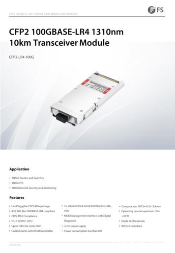
CFP2 100GBASE-LR4 1310nm 10km Transceiver Module . - FS
CFP2 100GBASE-LR4 1310NM 10KM TRANSCEIVER MODULECFP2 100GBASE-LR4 1310nm10km Transceiver ModuleCFP2-LR4-100GApplication 100GE Routers and Switches 100G OTN 100G Network Security And MonitoringFeatures Hot Pluggable CFP2 MSA package IEEE 802.3ba 100GBASE-LR4 compliant CFP2 MSA Compliance ITU-T G.959.1 2012 4 x 28G Electrical Serial Interface (CEI-28GVSR) MDIO management interface with DigitalDiagnostic Up to 10km for G.652 SMF 3.3V power supply Cooled 4x25G LAN-WDM transmitter Power consumption less than 6Wwww.fs.com Compact size: 107.5 41.5 12.4 mm Operating case temperature: -5 to 70 Duple LC Receptacle ROHs-6 compliant1
CFP2 100GBASE-LR4 1310NM 10KM TRANSCEIVER MODULEDescriptionFS's CFP2-100G-LR4 transceivers are designed for use in 100 Gigabit Ethernet links over 10km single module fiber, and it compliant tothe CFP MSA CFP2 HW Specification and IEEE 802.3ba 100GBASE-LR4. Digital diagnostics are available via MDIO as specified in the CFPMSA Management Interface Specification.The transceiver's designs are optimized for high performance and cost efficiency to provide customers the best solutions for Datacomand Telecom applications.The transceiver is RoHS-6 compliant and lead-free per Directive 2002/95/EC.Product SpecificationsI. Absolute Maximum RatingsThe limit of the maximum value is shown as below Table 1. (If operating out the limit of the maximum value will cause permanentdamage).ParameterSymbol ConditionsStorage temperature(case)TstgRelative humidityRHDamage Threshold for ReceiverPmaxMin.MaxUnit-40 85 85% 10.0dBm 3.6V0Vcc 3.3V-0.3Ref.Power SupplyVcc 5.0VVInput 3.3V LVCMOS signal levelVi-0.3Vcc 0.3VInput 1.2V LVCMOS signal levelVi-0.31.6V2000VESD Sensitivity on module and allhost pinswww.fs.comHBMHuman BodymodelR 1.5K,C 100pF2
CFP2 100GBASE-LR4 1310NM 10KM TRANSCEIVER MODULEII. Recommended Operating EnvironmentThe recommended working conditions are shown as below Table 2.ParameterSymbolMin.Operating Case TemperatureTc0Supply voltageVcc 3.3V 3.14Power dissipationTyp.Max.Unit 70 3.47VP6WLow Power dissipationPLow1WIn-rush CurentI-inrush200mA/usTurn-off rush CurentI-turnoff-200Link DistanceL2M 3.3Ref.mA/us10kmG.652 SMFIII. Optical CharacteristicsTable 3 -100Gb/s CFP2 Optical Specifications UnitTransmitterChannel data rate25.7812GbpsAggregate data rate103.125GbpsData rate variation-100 091309.141310.19nm10.5dBm4.5dBmLane Center WavelengthTotal Average Launch PowerPoutAverage Launch Power per LanePeachwww.fs.com-4.33
CFP2 100GBASE-LR4 1310NM 10KM TRANSCEIVER MODULEOptical Modulation Amplitude perLaneOMA-1.3Difference in Launch powerbetween any two lances(OMA)4.5dBm5.0dBLaunch power in OMA minus TDP,per lanePoma tdpAverage Launch Power of TX DISTransmitter per lanePoffExtinction RatioER4dBSMSRSMSR30dBDispersion PenaltyDP10km SMF2.2dBRelative Intensity NoiseRINMod off-130dB/HzOpitcal Return Loss ToleranceTRL20dBTransmitter reflectanceTef-12dBOptical Eye Mask {X1, X2, X3, Y1,Y2, Y3}1EM-2.3dBmTX DIS H-30dBm{0.25, 0.4, 0.45, 0.25, 0.28,0.4}ReceiverChannel data rate25.7812Data rate variation-100Gbps 091309.141310.19nmLane Center WavelengthDamage thresholdPDTAverage receiver power per laneRpowReceive power OMA per LaneRovlDifference in receive powerbetween any two lanes(OMA)Receiver Sensitivity(OMA) 8.6dBm4
CFP2 100GBASE-LR4 1310NM 10KM TRANSCEIVER MODULEStressed Receiver Sensitivity perLanePsen str-6.8dBmReceiver ReflectanceRef-26dBVertical eye closure penalty perLane1.8dBStressed eye jitter per Lane0.3UIConditions of stressed receiver sensitivity testRx-Lane LOS Assert-25Rx-Lane LOS De-assertRx-Lane LOS HysteresisdBm-130.5dBmdBNote1. Please refer to Figure 1Figure 1 - Transmission eye mask definitionwww.fs.com5
CFP2 100GBASE-LR4 1310NM 10KM TRANSCEIVER MODULETable 4 -100Gb/s CFP2 Optical Specifications smitterChannel data rate27.9525GbpsAggregate data rate111.809GbpsData rate variation-20 91309.141310.19nmLane Center WavelengthTotal Average Launch PowerPoutAverage Launch Power per LanePeachOptical Modulation Amplitudeper LaneOMA8.9dBm-2.52.9dBm-1.24.5dBmDifference in Launch powerbetween any two lances(OMA)5.0dBAverage Launch Power of TX DISTransmitter per lanePoffExtinction RatioER7dBSMSRSMSR30dBRelative Intensity NoiseRINOpitcal Return Loss ToleranceTRL20dBTransmitter reflectanceTef-12dBOptical Eye Mask {X1, X2, X3, Y1,Y2, Y3}1EMwww.fs.comTX DIS H-30Mod off-130dBmdB/Hz{0.25, 0.4, 0.45, 0.25, 0.28,0.4}6
CFP2 100GBASE-LR4 1310NM 10KM TRANSCEIVER MODULEReceiverChannel data rate27.9525Data rate variation-20Gbps 91309.141310.19nmLane Center WavelengthDamage thresholdPDTAverage receiver power per laneRpow4.5dBmReceiver power OMA per laneRovl4.5dBmDifference in receive powerbetween any two lanes(OMA)5.5dBOptical path penalty1.5dB5.5dBmReceiver Sensitivity per lane2Psen-10.3dBmReceiver Sensitivity(OMA) perlane2Psen OMA-9.1dBmReceiver ReflectanceRef-26dBRx-Lane LOS Assert-25Rx-Lane LOS DeassertRx-Lane LOS HysteresisdBm-130.5dBmdBNote1. Please refer to Figure 1Note2. OTU-4 Rate, BER 10-12 with FEC, ER 7dBwww.fs.com7
CFP2 100GBASE-LR4 1310NM 10KM TRANSCEIVER MODULEIV. Electrical CharacteristicsTable 5 - 100Gb/s CFP2 Electrical High Speed I/O Interface UnitTransmitter (CAUI input interface)Signal Rate Per Lane25.78125Signal Rate Tolerance-100AC Common ModeinputVoltage Tolerance(RMS)IEEE 802.3ba2010Gb/s100ppm20mVDifferential input return lossRldiffTotal Input Jitter ToleranceTjin0.62UIDeterministic Input Tolerance-JitterTdin0.42UISee Equation (83B–7)dBTransmitter Input Mask(X1, X2)-Eye(0.31, 0.5)UI1Transmitter Input Mask(Y1, Y2)-Eye(42.5, 425)mV1Receiver (CAUI output interface)Signal Rate Per Lane25.78125Signal Rate ToleranceSingle-ended output voltageVosigOutput AC commonmodevoltage(RMS)VocomACOutput transition timeTr20% 80%IEEE802.3ba2010Differential output returnlossGb/s-100100ppm-0.44V15mV24psSee Equation (83B–5)dBTotal JitterTj0.4UIDeterministic JitterTdj0.25UIwww.fs.com8
CFP2 100GBASE-LR4 1310NM 10KM TRANSCEIVER MODULEReceiver Output Eye Mask(X1,X2)(0.2, 0.5)UI2Receiver Output Eye Mask(Y1,Y2)(136, 380)mV2Note1. refer to figure 2Note2. refer to figure 3Figure 3 - CAUI transmitter eye maskLow Speed I/O interfaceTable 6 -100Gb/s CFP2 3.3V LVCMOS Electrical CharacteristicsMin.Typ.Vcc3.23.3Input High VoltageVIH2Input Low VoltageVIL-0.30.8VInput Leakage CurrentIIN-10 10mAOutput High Voltage (IOH 100uA)VOHVcc-0.2www.fs.comParameterSymbolSupply VoltageConditionMax.3.4Vcc 0.3Vcc 0.3UnitVVV9
CFP2 100GBASE-LR4 1310NM 10KM TRANSCEIVER MODULEOutput Low Voltage (IOL 100uA)VOL-0.3Minimum Pulse Width ofControl Pin Signalt CNTL1000.2VusNote:(MOD RSTn,MOD LOPWR,TX DIS,PRG CNTL,MOD ABS,RX LOS,GLB ALRMn, PRG ALRM ) are LVCMOS I/O interfaces.Table 7 - 100Gb/s CFP 1.2V LVCMOS Electrical .Input High VoltageVIH0.841.5VInput Low VoltageVIL-0.30.36VInput Leakage CurrentIIN-100Output High VoltageVOH1.01.5VOutput Low VoltageVOL-0.30.2VOutput High CurrentIOH-4mAOutput Low CurrentIOLInput capacitanceCi 100 4UnituAmA10pFMax.Unitt MOD LOPWR assert1msMOD LOPWR De- t MOD LOPWR deassertassert10s100usNote:(MDIO, MDC, PRTADR4:0) are 1.2V LVCMOS I/O interfacesTable 8 - 100Gb/s CFP Timing Parameters for CFP2 Hardware Signal PinsParameterHardwareMOD LOPWRassertHardwareReceiver Loss of Signal AssertTimewww.fs.comSymbolt loss assertConditionMin.Typ.10
CFP2 100GBASE-LR4 1310NM 10KM TRANSCEIVER MODULEReceiver Loss of Signal DeAssert Timet loss deassert100usGLB ALRMn assert150msGlobal Alarm De-AssertDelay GLB ALRMn deassertTime150msGlobal Alarm Assert DelayTimeManagement InterfaceClockPeriodt prd250nsHost MDIO t setupt setup10nsHost MDIO t holdt hold10nsCFP MDIO t delayt delay0Initialization time from Reset175nst initialize2.5sTransmitter Disabled(TX DISasserted)t de-assert100usTransmitter Enabled(TX DISde-asserted)t assert2msTable 9 - 100Gb/s CFP MDIO and MDC Timing CharacteristicsParameterSymbolManagement Interface ClockFrequencyF MDCManagement Interface ClockPeriodMax.Unit0.14MHzt prd25010000Host MDIO t setupt setup10nsHost MDIO t holdt hold10nsCFP MDIO t delay1t delay0175ns4060%MDC high and low timeConditionMin.www.fs.comnstwidth160MDIO/MDC termination in CFPTyp.Zt100nskOhm11
CFP2 100GBASE-LR4 1310NM 10KM TRANSCEIVER MODULENote1. Delay from MDC rising edge to MDIO data changeFigure 4 -100Gb/s CFP MDIO & MDC Timing DiagramClock interfaceTable 10 - 100Gb/s CFP Reference Clock Min.Typ.Max.Unit80100120ohm-100 100ppm1-20 ency Stability1/64 of host lane rateXfInput Differential VoltageVdiffRMS JitterσClock Duty CycleClock Rise/Fall Time 10/90%Tr/fNote1. For Ethernet applications Note2. For Telecom applicationsNote3. Peak to Peak DifferentialNote4. Random Jitter. Over frequency band of 10kHz f 10MHzNote5. 1/64 of electrical lanewww.fs.com12
CFP2 100GBASE-LR4 1310NM 10KM TRANSCEIVER MODULETable 11 - 100Gb/s CFP Transmitter & Receiver Monitor Clock Min.Typ.80100FrequencyOuput Differential VoltageMax.120Unitohm1/8 of network lane rateVdiffClock Duty Cycle40040120060mV1%Note1. Peak to Peak DifferentialV. 100Gb/s CFP Function DiagramInternal reference structureThe internal structure of 100Gb/s CFP shown as Figure 5.Figure 5 -10km 100Gb/s CFP2 internal structurewww.fs.com13
CFP2 100GBASE-LR4 1310NM 10KM TRANSCEIVER MODULEVI.Recommended Interface CircuitFigure 6 - Recommended High Speed I/O for Data and ClocksFigure 7 - Recommended MDIO Interface Terminationwww.fs.com14
CFP2 100GBASE-LR4 1310NM 10KM TRANSCEIVER MODULEVII.Pin LayoutFigure 8 - CFP2 Module Pad Layoutwww.fs.com15
CFP2 100GBASE-LR4 1310NM 10KM TRANSCEIVER MODULECFP2 Bottomwww.fs.comCFP2 Top1GND104GND2(TX MCLKn)103N.C.3(TX V GND98GND83.3V 3N.C.133.3V GND92GND143.3V GND91N.C.15VND IO A90N.C.16VND IO B89GND17PRG CNTL188TX1n18PRG CNTL287TX1p19PRG CNTL386GND16
CFP2 100GBASE-LR4 1310NM 10KM TRANSCEIVER MODULEwww.fs.com20PRG ALRM185TX0n21PRG ALRM284TX0p22PRG ALRM383GND23GND82N.C.24TX DIS81N.C.25RX LOS80GND26MOD LOPWR79(REFCLKn)27MOD ABS78(REFCLKp)28MOD RSTn77GND29GLB DR072RX3p34PRTADR171GND35PRTADR270RX2n36VND IO C69RX2p37VND IO D68GND38VND IO E67N.C.393.3V GND66N.C.403.3V GND65GND17
CFP2 100GBASE-LR4 1310NM 10KM TRANSCEIVER X1n453.3V GND60RX1p463.3V GND59GND47N.C.58RX0n48N.C.57RX0p49GND56GND50(RX MCLKn)55N.C.51(RX MCLKp)54N.C.52GND53GNDFigure 8 - CFP2 Module Pin MapNote1:Pin 15,16,36,37,38, are internally used and NOT allowed to connect any signal and power supply or GNDNote2: Pin 2,3,50,51 are disabled unless MCLK output is enabled via MDIOVIII.Pin DefinitionTable 12 - 100Gb/s CFP2 Pin Definition(Bottom raw)PINNameI/OLogicDescription1GND2(TX MCLKn)OCMLNot Support3(TX MCLKp)OCMLNot Support4GNDwww.fs.com18
CFP2 100GBASE-LR4 1310NM 10KM TRANSCEIVER MODULE5N.CNo Connect6N.CNo Connect73.3V GND3.3V Module Supply Voltage Return Ground,can be separate or tied together with Signal83.3V GNDGround93.3V3.3V Module Supply Voltage103.3V3.3V Module Supply Voltage113.3V3.3V Module Supply Voltage123.3V3.3V Module Supply Voltage133.3V GND143.3V GND15VND IO AI/O16VND IO BI/OModule Vendor I/O. Must No Connect at hostboardModule Vendor I/O. Must No Connect at hostboardProgrammable Control 1 set over MDIO, MSADefault: TRXIC RSTn, TX & RX ICs reset, "0":17PRG CNTL1ILVCMOSw/ PURreset, "1" or NC: enabled not used4.75kohmpull up in the moduleProgrammable Control 2 set over MDIO, MSADefault: Hardware Interlock LSB, "00": 3W,18PRG CNTL2ILVCMOSw/ PUR"01": 6W, "10": 9W, "11" or NC: 12W notused4.75kohm pull up in the moduleProgrammable Control 3 set over MDIO, MSADefault: Hardware Interlock MSB, "00": 3W,19PRG CNTL3ILVCMOSw/ PUR"01": 6W, "10": 9W, "11" or NC: 12W notused 4.75kohm pull up in the modulewww.fs.com19
CFP2 100GBASE-LR4 1310NM 10KM TRANSCEIVER MODULEProgrammable Alarm 1 set over MDIO, MSADefault: HIPWR ON, "1": module power up20PRG ALRM1OLVCMOScompleted, "0":module not high poweredupProgrammable Alarm 2 set over MDIO, MSA21PRG ALRM2OLVCMOSDefault:MOD READY, "1": Ready, "0": notReady.Programmable Alarm 3 set over MDIO, MSA22PRG ALRM3OLVCMOSDefault: MOD FAULT, fault detected, "1":Fault, "0": No Fault23GNDTransmitter Disable for all lanes,"1" or NC 24TX DISILVCMOSw/ PURtransmitter disabled, "0" transmitterenabled25RX LOSOLVCMOSReceiver Loss of Optical Signal, "1": lowopticalsignal, "0": normal conditionModule Low Power Mode."1" or NC:module in low power (safe) mode, "0":26MOD LOPWRILVCMOSw/ PURpower-on enabled4.75kohm pull up in themoduleModule Absent. "1" or NC: module absent,27MOD ABSOGND"0":module present, Pull Up Resistor onHostModule Reset. "0" resets the module, "1" or28MOD RSTnILVCMOSw/ PDRNC module enabled, 4.75kohm pull downin the moduleGlobal Alarm. “0": alarm condition in anyMDIO Alarm register, "1": no alarm29GLB ALRMnOLVCMOScondition, Open Drain, Pull Up Resistor onHostwww.fs.com30GND31MDCI1.2V CMOSManagement Data Clock (electrical specs asper 802.3ae and ba)20
CFP2 100GBASE-LR4 1310NM 10KM TRANSCEIVER MODULEManagement Data I/O bi-directional data32MDIOI/O1.2V CMOS33PRTADR0I1.2V CMOSMDIO Physical Port address bit 034PRTADR1I1.2V CMOSMDIO Physical Port address bit 135PRTADR2I1.2V CMOSMDIO Physical Port address bit 236VND IO CI/OModule Vendor I/O C. Do Not Connect!37VND IO DI/OModule Vendor I/O D. Do Not Connect!38VND IO EI/OModule Vendor I/O E. Do Not Connect!393.3V GND403.3V GND413.3V423.3V433.3V443.3V453.3V GND463.3V GND47N.CNo Connect48N.CNo Connect49GND50(RX MCLKn)(electrical specs as per 802.3ae and ba)3.3V Module Supply Voltagewww.fs.comOCMLNot Support21
CFP2 100GBASE-LR4 1310NM 10KM TRANSCEIVER MODULE51(RX MCLKp)52GNDOCMLNot SupportTable 13 -100Gb/s CFP2 Pin Definition(Top raw)PINName53GND54N.CNo Connect55N.CNo Connect56GND57RX0pOHS I/OLane 0 Receiver Output (Positive)58RX0nOHS I/OLane 0 Receiver Output (Negative)59GND60RX1pOHS I/OLane 1 Receiver Output (Positive)61RX1nOHS I/OLane 1 Receiver Output (Negative)62GND63N.CNo Connect64N.CNo Connect65GND66N.CNo Connect67N.CNo Connect68GND69RX2pwww.fs.comI/OOLogicHS I/ODescriptionLane 2 Receiver Output (Positive)22
CFP2 100GBASE-LR4 1310NM 10KM TRANSCEIVER MODULEwww.fs.com70RX2nOHS I/OLane 2 Receiver Output (Negative)71GND72RX3pOHS I/OLane 3 Receiver Output (Positive)73RX3nOHS I/OLane 3 Receiver Output (Negative)74GND75N.CNo Connect76N.CNo Connect77GND78REFCLKpIReference Clock Input (Positive), optional79REFCLKnIReference Clock Input (Negative) , optional80GND81N.CNo Connect82N.CNo Connect83GND84TX0pIHS I/OLane 0 Transmitter Input (Positive)85TX0nIHS I/OLane 0 Transmitter Input (Negative)86GND87TX1pIHS I/OLane 1 Transmitter Input (Positive)88TX1nIHS I/OLane 1 Transmitter Input (Negative)89GND90N.CNo Connect23
CFP2 100GBASE-LR4 1310NM 10KM TRANSCEIVER MODULE91N.C92GND93N.CNo Connect94N.CNo Connect95GND96TX2pIHS I/OLane 2 Transmitter Input (Positive)97TX2nIHS I/OLane 2 Transmitter Input (Negative)98GND99TX3pIHS I/OLane 3 Transmitter Input (Positive)100TX3nIHS I/OLane 3 Transmitter Input (Negative)101GND102N.CNo Connect103N.CNo Connect104GNDwww.fs.comNo Connect24
CFP2 100GBASE-LR4 1310NM 10KM TRANSCEIVER MODULEIX. 100Gb/s CFP Mechanical Specifications100Gb/s CFP2 mechanical dimensions should be compliant with CFP2 MSA specification.Detailed dimensions are shown in Figure 10.Figure 10 - 100Gb/s CFP2 Mechanical Dimensions(unit:mm)X. Management InterfaceCFP2-100G-LR4 transceivers support the MDIO interface specified in IEEE802.3 Clause 45. This 2-wire management data I/O interfaceis provided for the module status monitoring and control. The management data clock (MDC) provides clocking for the data that ispassed on the MDIO port. Five further pins allow for loading of a port address (PORT ADDR0-4) into the module.Figure 12 - CFP MDIO Interfacewww.fs.com25
CFP2 100GBASE-LR4 1310NM 10KM TRANSCEIVER MODULETest CenterI. Compatibility TestingEach fiber optical transceiver has been tested in host device on site in FS Assured Program to ensure full compatibility with over 200vendors.Cisco Catalyst C9500-24Y4CBrocade VDX 6940-144SForce⑩tm S6044TCisco MS425-16Dell EMC Networking Z9100-ONHUAWEI S6720-30L-HI-24SAbove is part of our test bed network equipment. For more information, please click the Test Bed PDF. It will be updated in real time aswe expand our portfolio.www.fs.com26
CFP2 100GBASE-LR4 1310NM 10KM TRANSCEIVER MODULEII. Performance TestingEach fiber optical transceiver has been fully tested in FS Assured Program equipped with world's most advanced analyticalequipment to ensure that our transceivers work perfectly on your device.1. TX/RX Single Quality TestingEquipped with the all-in-one tester integrated 4ch BERT & samplingoscilloscope, and variable optical attenuator the input and output signalquality. Eye Pattern Measurements: Jitter, Mask Margin, etc Average Output Power OMA Extinction Ratio Receiver Sensitivity BER Curve2. Reliability and Stability TestingSubject the transceivers to dramatic in temperature on the thermal shockchamber to ensure reliability and stability of the transceivers. Commercial: 0 to 70 Extended: -5 to 85 Industrial: -40 to 85 3. Transfer Rate and Protocol TestingTest the actual transfer data rate and the transmission ability under differentprotocols with Networks Master Pro. Ethernet Fiber Channel SDH/SONET CPRI4. Optical Spectrum EvaluationEvaluate various important parameters with the Optical Spectrum Analyzerto meet the industry standards. Center Wavelength, Level OSNR SMSR Spectrum Widthwww.fs.com27
CFP2 100GBASE-LR4 1310NM 10KM TRANSCEIVER MODULEOrder InformationPart NumberDescriptionCFP-SR10-100GCFP 100GBASE-SR10 850nm 150m Transceiver ModuleCFP-LR4-100GCFP 100GBASE-LR4 1310nm 10km Transceiver ModuleCFP-ER4-100GCFP 100GBASE-ER4 1310nm 40km Transceiver ModuleCFP2-LR4-100GCFP2 100GBASE-LR4 1310nm 10km Transceiver ModuleCFP4-LR4-100GCFP4 100GBASE-LR4 1310nm 10km Transceiver ModuleCXP-SR10-100GCXP 100GBASE-SR10 850nm 150m Transceiver Modulewww.fs.com28
United KingdomUnited StatesRussiaGermanyChinaSingaporeAustraliaAll statements, technical information, and recommendations related to the products here are based upon information believedto be reliable or accurate. However, the accuracy or completeness thereof is not guaranteed, and no responsibility is assumed forany inaccuracies. Please contact FS for more information.Copyright 2009-2020 FS.COM All Rights Reserved.
R 1.5K,C 100p F 2000 V CFP2 100GBASE-LR4 1310NM 10KM TRANSCEIVER MODULE Description FS's CFP2-100G-LR4 transceivers are designed for use in 100 Gigabit Ethernet links over 10km single module fiber, and it compliant to the CFP MSA CFP2 HW Specification and IEEE 802.3ba 100GBASE-LR4. Digital diagnostics are available via MDIO as specified in the CFP
42 53.13 Wendy Wise 10km - 50 to 59 Female 43 53.23 Jade Regan 10km - Under 16 Female 44 53.27 Kara Curphey 10km - 40 to 49 Female 45 53.47 Jeremy Norton 10km - Open Male 46 53.51 Tanya Buckingham 10km - 40 to 49 Female Backyard Bootcamp 47 54.00 Tom Docherty 10km - Open Male M
BiDi CFP2-DCO is a digital coherent module designed for bi-directional single-fiber transmission. It is the first digital coherent module in the industry to successfully integrate rich DSP and FEC options, two independently tuned narrow-linewidth lasers, and an optical EDFA in a CFP2 form factor. In addition, BiDi CFP2-DCO is
NBNSYS0000005163 Balaenoptera musculus Blue whale Calving/nursing Location of adults, females with calves 10km 10km Disturbance NHMSYS0000376882 Balaena mysticetus Bowhead whale Calving/nursing Location of adults, females with calves 10km 10km Disturbance NBNSYS0000005179 Tursiops truncatus Common bottlenosed dolphin
Introduction This describes a possible baseline proposal for a new 4-lane interleaved 100G FEC sublayer for P802.3ck This new FEC sublayer could be used along with existing Clause 82 PCS and revised Clause 135 PMA to support the objectives for the 100GBASE-KR1 and 100GBASE-CR1 channels The intent of the presentation is not to propose the use of interleaved FEC for
transimpedance amplifier running out of headroom . Differential output return loss as R matching See 86A.4.1.1 — dB Eqn. A-1 — Eqn. A-1 — Common-mode output return loss See 86A.4.1.2 — dB Eqn. A-2 — Eqn. A-2 — Unwisely deleted from 802.3- 2012 Common-mode to
Figure 14: Return Loss versus CEI-28G-VSR Mask Requirements Figure 15: Mode Conversion versus CEI-28G-VSR Mask Requirements Design Guidelines for 100 Gbps - CFP2 Interface Altera Corporation Feedback Simulation Results for Stratix
2010-2013 RANGE ROVER SPORT & LAND ROVER LR4 REMOTE STARTER INSTALLATION INSTRUCTIONS During your first installation of this product, you will benefit from these complete instructions. After performing two or three, you should only need the Wire Connections Page. The entire installation is inside the vehicle, on the passenger side.
API 541 5th Edition - Scope This standard covers the minimum requirements for special purpose form-wound squirrel-cage induction motors 375 kW (500 Horsepower) and larger for use in petroleum, chemical and other industry applications. Note 1: Special purpose machines typically have one or more of the following characteristics: 1. Is in an .


