RFMS 2020: Connector To PCB Interface - Molex
RFMS 2020: Connector to PCB InterfaceJean Louis MendesBDM/FEA RF & MicrowaveE-mail:Jeanlouis.mendes@molex.comMolex Confidential InformationMobile: 4670 59464 Reserved. Unauthorized Reproduction/Distribution is Prohibited.1 Molex,LLC –57All Rights
Interface Analysis PCB Analysis Connector interface Analysis— PCB Launch effect RF Performances improvement Conclusion2Molex Confidential Information Molex, LLC – All Rights Reserved. Unauthorized Reproduction/Distribution is Prohibited.
PCB Analysis SMPM Connector (73300044x)— Frequency up to 30GHz PCB— Dielectric : Megatron6 Er 3.6 TanDelta 0.002 Simulation HFSS3PCB Strucure25 um75 um due to Layer 1 impedance25 um205 um due to Pad Width25 um400 um due to PCB StudyMolex Confidential Information Molex, LLC – All Rights Reserved. Unauthorized Reproduction/Distribution is Prohibited.Layer 1Diel 1Layer2Diel 2Layer3Diel 3Layer4
50Ω Line simulationLine WidthL1 thicknessD1 thicknessGND ClearenceGND ClearenceLine WidthLayer 1 GND ClearenceDiel 1L1 ThicknessLayer 2 D1 ThicknessErCalculated Impedance135um200um25um75um3.46um49.7OhmLine Length 20mmImpedance is 50OhmIL below 0.6 dB up to 30GHzRL below -35dB up to 30GHz4Molex Confidential Information Molex, LLC – All Rights Reserved. Unauthorized Reproduction/Distribution is Prohibited.
50Ω Line simulationSMPM Design 2SMPM connectorLine WidthL1 thicknessD1 thickness Connector Placed directly on PCBRL below-15dB5RL above-10dBMolex Confidential Information Molex, LLC – All Rights Reserved. Unauthorized Reproduction/Distribution is Prohibited.GND ClearenceGND ClearenceLine WidthLayer 1 GND ClearenceDiel 1L1 ThicknessLayer 2 D1 ThicknessErCalculated Impedance150um200um25um75um3.46um49.7OhmClipping PlaneThe first effect is due to Pad width.Some opening has to be done in order tokeep a 50Ohm structure
50Ω Line simulationSMPM Design 3add Diel-2 100 umThicknessAnd perform openingConnector Hided21 Opening done on layer 2SMPM connectorPAD WidthL1 thicknessD1 thicknessL2 Thickness6GND ClearenceGND ClearenceLine WidthGND ClearenceLayer 1 L1 ThicknessDiel 1D1 ThicknessLayer 2 L2 ThicknessD2 ThicknessTotal ThicknessErCalculated ImpedanceClipping Plane1Layer 1Layer 2Layer 3550um200um25um75um25um200Um300um3.4649.7OhmMolex Confidential Information Molex, LLC – All Rights Reserved. Unauthorized Reproduction/Distribution is Prohibited.2By Opening Layer 2 we improve:1. the line response2. We improve the overall responseBut it’s Not Enough
50Ω Line simulationSMPM Design 4add Diel-3 100 umThicknessAnd add openingConnector Hided21Clipping Plane Opening done on layer 2SMPM connectorLine Width700umGND Clearence200umGND ClearenceGND ClearenceLayer 1 L1 Thickness25umDiel 1D1 Thickness75umLayer 1 L2 Thickness25umDiel 1D2 Thickness200umLayer 1 L3 Thickness25umDiel 1D3 Thickness100umTotal thickness400umEr3.46Molex Confidential InformationCalculated Impedance49.7Ohm Molex, LLC – All Rights Reserved. Unauthorized Reproduction/Distributionis Prohibited.PAD WidthL1 thicknessD1 thicknessL2 ThicknessD2L3D3L47Layer 1Layer 2Layer 3Layer 4Could be compareat stripLine12By Opening Layer 2 and 3 Weimprove:1. The line response again2. The overall responseBut it’s still Not EnoughFrom now need to knowwhat is inside the connector
50Ω Line simulationSMPM Design 5Increase Diel-3 ThicknessConnector Hided21Clipping PlaneSMPM connectorL1 thicknessD1 thicknessL2 ThicknessD2L3D3L48GND ClearenceGND ClearenceCould be compareat stripLine1 Opening done on layer 2PAD WidthLayer 1Layer 2Layer 3Layer 4Line WidthGND ClearenceLayer 1 L1 ThicknessDiel 1D1 ThicknessLayer 1 L2 ThicknessDiel 1D2 ThicknessLayer 1 L3 ThicknessDiel 1D3 ThicknessTotal thicknessErCalculated 3.4649.7OhmMolex Confidential Information Molex, LLC – All Rights Reserved. Unauthorized Reproduction/Distribution is Prohibited.2By increasing the dielectric Thickness:1. We improve the line responseagain2. We open even more the dielectricbelow the Connector we improvethe overall responseFrom now need to knowwhat is inside the connector
50Ω Line simulationSMPM Design 6Some option for improving RLConnector Hided21Clipping Plane Opening done on layer 2SMPM connectorL1 thicknessD1 thicknessL2 ThicknessD2L3D3L49Line Width700umPAD WidthGND Clearence200umGND ClearenceGND ClearenceLayer 1 L1 Thickness25umDiel 1D1 Thickness75umLayer 1 L2 Thickness25umDiel 1D2 Thickness200umLayer 1 L3 Thickness25umDiel 1D3 Thickness200umTotal thickness500umEr3.46Molex Confidential InformationCalculated Impedance49.7Ohm Molex, LLC – All Rights Reserved. Unauthorized Reproduction/Distributionis Prohibited.Layer 1Layer 2Layer 3Layer 4Could be compareas stripLine12By Filtering1. We improve the simulationresponse again2. By closing partially theopening we didn’t improve somuch the simulation response.But we improve the RFperformances (next slide)For further improvement: We need toknow the “inside” of the connector
RF Performance The Red Line is from Design 6 (Filter)RL has been degrade around 10GHzBut the Interface response has improvedabove 20GHz10Molex Confidential Information Molex, LLC – All Rights Reserved. Unauthorized Reproduction/Distribution is Prohibited.
Some Other Parameter To Play2/ Opening Distance1/ GND ClearenceThe Customer Should KnowOur Team is Ready to help. Help to design and/or optimizethe PCB launch for you3/ Opening Thickness11Molex Confidential Information Molex, LLC – All Rights Reserved. Unauthorized Reproduction/Distribution is Prohibited.
Molex Confidential Informationregisteredof Reserved.Molex, LLCUnauthorizedin the United Statesof America and mayisbeProhibited.registered in other countries; all other trademarks listed herein belong to their respective owners.12Molex is aMolex,LLCtrademark– All RightsReproduction/Distribution
RFMS 2020: Connector to PCB Interface Author: O'
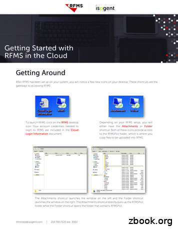
RFMS in the Cloud rfmshelp@isogent.com 214.790.7220 ext. 3002 Getting Around Depending on your RFMS setup, you will either have the Attachments or Folder shortcut. Both of these icons provide access to the RFMSPict folder, which is where you copy files to be uploaded into RFMS. To launch RFMS, click on the RFMS desktop icon.
open RFMS. This is the screen you should see when you first launch RFMS. From this screen, click on Order Entry. The RFMS Order Entry screen will pull up. On page 3 of the RFMS Cloud Workbook, we ask that you attach a screenshot of the RFMS System Information Screen with the completed workbook. Getti
RFMS User Manual Ver 6 1.1 RFMS Features RFMS facilitate ministries/departments to prepare RFD online and input achievements. Access to RFMS is restricted to officials nominated by Departments and is granted through UserId/Password. Access is Role based. The Roles can be created by Perfor
SP3 : Technologies de traitement SP4 : Outil global d'aide à la décision Action 6 PCB OPTITRI Action 7 PCB ECODEPOT Action 8 STAB PCB Action 9 PCB SEDICA Action 10 FUNGI EAT PCB Action 12 BIODECHLOR PCB Action 13 DESTHER PCB Action 14 PLATPIL PCB Action 15 SEDIRHONE PCB / / / / SP3.1 : dragage et criblage SP3.2 : confinement SP3.3 : absorption
RFMS benefits Contact us Overview ONLINE The Resident Fund Management Service (RFMS) is a financial service offered by National Datacare Corporation and a participating financial institution. It is a state-of-the-art, online fund management system for managing your resident trust fund account. RFMS benefits Contact us
11.1 PCB design process The PCB Design training covers how to use the PCB Editor to create a PCB from setup, through component placement, routing, design rule checking and CAM output. We first look at the overall PCB design process. The diagram below shows an overview of the PCB design process from schematic entry through to PCB design completion.
Aluminum Single Side PCB Aluminum Metal Clad Circuit Boards Aluminum Printed Circuit Board P r o d u c t s & S e r v i c e s. MC PCBS MC PCB Single Slide PCB SS PCB Panel Light MC PCB P r o d u c t s & S e r v i c e s. METAL CORE PCBS LED Street Lights Metal Clad PCB Metal Clad PCB Metal Core Circuit Metal Core Circuit Boards P r o d u c t s .
Baking spread gives excellent results in cakes – choose a spread with a minimum 58% fat. If you prefer to use butter or packet margarine, it’s important that it’s at the right consistency – it should be soft and squishy but not oily. Mary Berry’s Perfect Victoria Sandwich The traditional Victoria Sandwich is a baking classic and a tasty teatime treat. This ‘all-in-one’ method is .


