SECTION 5: OPTICAL AMPLIFIERS
SECTION 5: OPTICAL AMPLIFIERS1
OPTICAL AMPLIFIERS· In order to transmit signals over long distances ( 100 km) it is necessary tocompensate for attenuation losses within the fiber.· Initially this was accomplished with an optoelectronic module consisting of anoptical receiver, a regeneration and equalization system, and an opticaltransmitter to send the data.· Although functional this arrangement is limited by the optical to electrical andelectrical to optical ronic AmpEqualizationRegenerationOpticalSignalOut· Several types of optical amplifiers have since been demonstrated to replace theOE – electronic regeneration systems.· These systems eliminate the need for E-O and O-E conversions.· This is one of the main reasons for the success of today’s opticalcommunications systems.2
OPTICAL AMPLIFIERSThe general form of an optical iberOptical AMP MediumOpticalSignalOutOpticalSignalInSome types of OAs that have been demonstrated include:· Semiconductor optical amplifiers (SOAs)· Fiber Raman and Brillouin amplifiers· Rare earth doped fiber amplifiers (erbium – EDFA 1500 nm, praseodymium –PDFA 1300 nm)The most practical optical amplifiers to date include the SOA and EDFA types.New pumping methods and materials are also improving the performance ofRaman amplifiers.3
Characteristics of SOA types:· Polarization dependent – require polarization maintaining fiber· Relatively high gain 20 dB· Output saturation power 5-10 dBm· Large BW· Can operate at 800, 1300, and 1500 nm wavelength regions.· Compact and easily integrated with other devices· Can be integrated into arrays· High noise figure and cross-talk levels due to nonlinear phenomenon such as 4wave mixing.This last feature restricts the use of SOAs.· Semiconductor Optical Amplifier (SOA) – similar to a laser cavity. Used as adiscrete amplifiers. They can be integrated into arrays of amplifyingswitching and gating devices. Finding application in all optical 3Rregeneration systems.ARWeak OpticalSignal InElectricalDrive CurrentSemiconductor CavityARAmplified OpticalSignal· Limited in operation below 10 Gb/s. (Higher rates are possible with lowergain.)4
Rare Earth Doped Fiber Amplifier Characteristics:Rare earth doped fiber amplifiers are finding increasing importance in opticalcommunications systems. Perhaps the most important version is erbium dopedfiber amplifiers (EDFAs) due to their ability to amplify signals at the low loss 1.55mm wavelength range.Characteristics of EDFAs (advantages):· High power transfer efficiency from pump to signal power ( 50%).· Wide spectral band amplification with relative flat gain ( 20 dB) – useful forWDM applications.· Saturation output 1 mW (10 to 25 dBm).· Gain-time constant long ( 100 msec) to overcome patterning effects and intermodulation distortions ( low noise).· Large dynamic range.· Low noise figure.· Polarization independent.· Suitable for long-haul applications.Disadvantages of EDFAs:· Relatively large devices (km lengths of fiber) – not easily integrated with otherdevices.· ASE – amplified spontaneous emission. There is always some output even withno signal input due to some excitation of ions in the fiber – spontaneous noise.· Cross-talk effects.· Gain saturation effects.5
· An energy level diagram for Er doped silica is shown below.4I (11/2)0.98 um4I (13/2)1.53 umPumpBands1.48 umEmissionWavelengths4I (15/2)· Pumping is primarily done optically with the primary pump wavelengths at 1.48mm and 0.98 mm. As indicated atoms pumped to the 4I (11/2) 0.98 mm banddecays to the primary emission transition band. Pumping with 1.48 mm light isdirectly to the upper transition levels of the emission band.· Semiconductor lasers have been developed for both pump wavelengths.· 10-20 mW of absorbed pump power at these wavelengths can produce 30-40dB of amplifier gain.· Pump Efficiencies of 11 dB/mW achieved at 980 nm.· Pumping can also be performed at 820 and 670 nm with GaAlAs laser diodes.Pump efficiencies are lower but these lasers can be made with high outputpower.6
Typical Absorption/Gain Spectrum for Erbium Doped oss Section(X 10 (-25)m 2)101.55Wavelength (um)· Since the gain spectrum of erbium resembles a 3-level atom it is possible tomodel the gain properties using this approach.· Several different wavelength bands have been designated for wavelengthdivision multiplexing and EDFAs have been designed to operate in these bands.· The divisions have been designated as*:S-Band 1480-1520 nmC-Band 1521-1560 nmL-Band 1561-1620 nm(* Note some variability in these values is common.)7
General EDFA Amplifier Configuration:980 or 1480 pump laserAmplified OutputSignalIsolatorEDFAWeak InputSignalNarrow BandFilterCouplerBasic Amplifier CharacteristicsOptical Gain· Rare earth doped optical amplifiers work much like a laser.· The primary difference is that they do not have a resonator.· Amplification occurs primarily through the stimulated emission process.· The medium is pumped until a population inversion state is achieved. Pumppowers are typically several 20-250 mW. An isolator is used to reducereflections at the input to the amplifier. A narrow band optical filter is used toreduce transmission of amplified spontaneous emission frequency components.· The resultant optical gain depends both on the optical frequency and the localbeam intensity within the amplifier section.· For basic discussion consider a two-level homogeneously broadened medium.8
· The gain coefficient can be expressed as:g (w ) go1 (w - w o ) 2 T22 P / Ps,go is the peak gain, w is the optical frequency of the incident signal,wo is the transition frequency, P is the optical power of the incident signal,T2 is the dipole relaxation time, and Ps is the saturation power.· Typically T2 is small 1 ps, and the saturation power Ps depends on gainmedium parameters such as the fluorescence time and the transition crosssection.9
Gain Spectrum and BW:· When not saturated (i.e. P/Ps 1) the gain coefficient g(w) becomes:g (w ) go.1 (w - w o ) 2 T22· Gain is maximum when w wo (i.e. the gain coefficient is at resonance).· At non-resonant frequencies the gain follows the homogeneously broadenedcharacteristics of a two level atom (i.e. Lorentzian profile).· The gain BW for this spectrum is typically expressed as the (Full Width at HalfMaximum) FWHMDw g 2 T2 .Dn g Dw g2pwith T2 ; 0.1 psDn g ; 3THz· Large Spectral BW amplifiers are preferred for fiber optic systems to makethem less sensitive to dispersed transmitted signals and useful for WDMsystems.EDFA Gain Spectrum:· The gain spectrum of erbium ions alone is homogeneously broadened and theBW is determined by the dipole relaxation time T2.· However when placed in a glass host the spectrum is influenced both by thesilica and any other dopants. This can result in inhomogeneous broadeningcontributions.· The combined homogeneous and inhomogeneous BW of EDFAs: 30 nm.10
Amplification factor:· Define as:G Pout/PinPout is the amplifier output power and Pin the input power of a CW input signal.PumpN2PinN1PGainMediumz 0outz L· From the previous discussion of the laser the gain in optical power per length ofgain medium (z) with gain g isdP gP .dz· Integrating over a length z of amplifier medium gives the resultant opticalpowerP( z ) P(0) exp( gz ) .11
The amplification factor after a length L of OAM (optical amplifier medium) isG (w ) exp[g (w ) L]Both g(w) and G(w) are a maximum when the frequency is at resonance w w oand decrease when the frequency is detuned from resonance.However the amplifier factor(G) decreases much faster than the gain coefficient(g).· The amplifier BW DnA is defined as the FWHM of G(w)æ ln 2 ö Dn A Dn g ççln(G/2)oøè0.5where Dng is the gain BW, and Go exp(goL).· The amplifier BW is smaller than the gain BW. The difference depends on theamplifier gain characteristics.If Go 10, Dn A 0.656 Dn g12
Gain Saturation:· Since g(w) depends on the incident optical power when P » PS, G will start todecrease with an increase in optical power P.· Assume that the incident frequency is tuned for peak gain (w wo)go PdP .dz 1 P / Ps· With the conditions P(0) Pinc and P(L) Pout GPinc the large signalamplifier gain becomesæ G - 1 PoutG Go expçç G PSèö .ø· This expression shows how the amplifier gain decreases when Pout » Ps.Output saturation power º the optical power at which G is reduced to Go/2 (3 dB)Psatout Go ln 2Ps .Go - 2· Typically Go 1000 (30 dB),s\ Pout» (ln 2) Ps » 0.69 Ps .13
Amplifier Noise:· Spontaneous emission in the amplifier will degrade the SNR by adding to thenoise during the amplification process.· SNR degradation is quantified through the amplifier noise figure FnFn (SNR )in(SNR )outwhere the SNR is based on the electrical power after converting the optical signalto an electrical current. Therefore Fn is referenced to the detection process anddepends on parameters such as detector bandwidth (Be) and thermal and shot noise.· Consider a simple case with an ideal detector with performance limited by shotnoise.· The amplifier has an amplification factor G (Pout G Pin).· SNR of the input signal:SNRin I2s s2(RPin )2 2q( RPin )Be Pin,2hnBes s2 2q (RPin )Be .· The spontaneous emission contribution is amplified along with the signal. TheSpectral density of the spontaneous emission induced noise is nearly constant(white noise) and can be expressed as:S sp (n ) (G - 1)n sp hn· Spontaneous emission population inversion factor nsp is given by:N2.N 2 - N1N2 and N1 are the population densities for the excited and ground states of theamplifying medium.n sp 14
· Alternatively can express the spontaneous emission power within the receiverbandwidth Be as:Psp 2 S sp Be· Spontaneous emission adds fluctuations to the amplified power and is convertedto current fluctuations at the detector output.· Major contribution to receiver noise results from coherent interference (beating)between the spontaneous emission with the signal. This results in a noisecurrent given byDI 2 R(GPin Psp )1/ 2 cos q· The variance in the photocurrent after the signal is passed through the amplifieriss 2 » 4( RGPin ) (RS sp )Bewhere cos2 q is replaced with its average value of ½. (Note that this relationassumes several idealizations on the detection process i.e. other noise sources arenegligible.)· The SNR of the amplified signal becomesSNRout (RGPin )2s2»GPin4 S sp Beand the amplifier noise figure isFn 2n sp (G - 1) / G » 2n sp .· For most amplifiers Fn 3 dB and can be 6-8 dB.15
· Characteristic plot of gain and noise figure for an erbium doped fiberamplifier pumped 30 mW at 980 nm.Noise Figure30302020101000151015201530Wavelength (nm)161540Gain (dB)4040
EDFA Gain Equalization10Loss/Gain(dB/m)UnflattenedEDFA Gain50FlattenedEDFA Gain1.511.531.55Wavelength (um)· Gain equalization can be accomplished in several ways:a. Thin film filtersb. Long period fiber gratingsc. Chirped fiber Bragg gratings171.56
Raman Scattering, Stimulated Raman Scattering, and Raman Amplifiers:· Raman scattering is an elastic scattering mechanism. Does not require apopulation inversion.· A photon with energy hn1 traveling through a material can excite avibrational transition of the material forming an optical phonon with energyhnp and a photon with slightly reduced energy hn2 given byEnergyn 2 n1 -n phn2hn1hnp· Molecule is raised to a new vibrational state and the energy of the photonis reduced.· There is a large difference between the photon and phonon energies.· Raman scattering is weak effect. It occurs through a slight modulation ofthe refractive index through molecular vibrations of the material.· Can derive the effect through a discussion of polarizability of a material.18
· The electric field induces a dipole moment of the moleculep qxorp aEwhere a is the complex polarizability of the molecule.xo q-qE· The bulk polarizability of a material is expressed asP eo c ( ) E1with c (1) the linear susceptibility of the material.· Response of a to an incident harmonic electric field:a ( x ) ao ¶a¶xdxxodx is the displacement from the equilibrium molecular length xod x ( t ) d xo e19 jw p t
p(t ) a (t ) E (t )æ¶a çao ç¶xè\d xo exo a o Eo e jw1t ¶a¶x jw p töjw t Eo e 1ød xo Eo e()j w1 w p txo· There are two frequency components: a) w1 ; b) w1 w p· The second component is nonlinear the output frequency is differentfrom the input 1hn2hnp· Scattered light with lower energy (n 2 n 1 ) Stokes Scattering.· Scattered light with higher energy (n 2 n 1 ) Anti-Stokes Scattering.· Stokes scattering typically dominates due to greater population of the groundstate relative to the vibrational state when the system is in thermalequilibrium.· At low illumination levels the Raman process results in low scattering levels.· The molecules contributing to the process are vibrating independently andthe scattered light is non-directional. Spontaneous Raman Scattering.20
· At higher intensity levels the generated photons begin to act in phase orcoherently – i.e. the molecules oscillate as an array of vibrating oscillators.This gives rise to Stimulated Raman Scattering (SRS).· SRS can be can be a problem but it can also be used as a signal amplificationprocess.· On the negative side it contributes to dispersion and places an operationallimit on the amount of power that can be transmitted through a fiber.· The Stokes wave is amplified as it propagates through the mediumdI 2 Gr I 2 I1dzI2 is the intensity of the Stokes shifted light (w s w1 - wvib ) ; I1 is the intensityof the pump beam (w1); and Gr is the Raman gain term that includes materialfactors such as ¶a / ¶x and varies as 1/l2.· For I2 I1 and cases where the pump beam is not significantly depleted:I 2 ( z ) I 2 ( 0 ) eGr I1 z21
Properties of Raman Amplifiers:Raman Gain Coefficient· The peak resonance in silica fibers occurs about 13 THz from the pumpwavelength. At 1550 nm this corresponds to a shift of about 100 nm.l p 1550 nm02413Frequency Shift (THz)· As indicated power is transferred from shorter wavelengths to longerwavelengths.· Coupling with the pump wavelength can be accomplished either in theforward or counter propagating direction.· Power is coupled from the pump only if the signal channel is sending a 1bit.22
Pump Arrangement to Extend the Range for Stimulated Raman Amplification:· An array of laser diodes can be used to provide the Raman pump. The beamsare combined and then coupled to the transmission fiber. The pump beamscan counter propagate to the direction of the signal beams.Transmission FiberRaman PumpBlockLaserDiodeArray14xx/1550 nmWDM Coupler1430 nm1450 nm1470 nm1490 nm2314xx nmCombiner
Difficulties with Raman Amplifiers:· The Pump and amplified signals are at different wavelengths. Thereforethe signal and the pump pulses will separate due to dispersion(waveguide dispersion) after a certain propagation distance. Thedifference in propagation time is given by:d t ( L / c ) l 2 d 2 n / d l 2 (d n / n )L is the fiber length.· A 1 psec pump pulse at 600 nm separates from a 1 psec Stokes pulse in 30 cm.· A second problem is that the pump power decreases along the fiberlength due to linear absorption and scattering – Raman gain is greater atthe input end.· A final problem results from amplifying spontaneous Raman photons.This occurs when the pump power is increased to offset attenuationlosses and spontaneous Raman photons are coupled into the guided modeall along the length of the fiber. This increases noise.· Upper limit on the power into a communications signal from SRSamplification can be defined as the point at which the Stokes power Prequals the signal power Psig.16p wo2P Gr LeffLeff1 - e -a L aExample:l p 1.55m mwo » 5m m Amod e » 80 m m2a linear » 0.2dB / km Leff » 20km 700 mWGr 9 10-12 m / WQUITE LARGE compared to normal optical signal powers ( 1 mW).24
Semiconductor optical amplifiers (SOAs) Fiber Raman and Brillouin amplifiers Rare earth doped fiber amplifiers (erbium – EDFA 1500 nm, praseodymium – PDFA 1300 nm) The most practical optical amplifiers to date include the SOA and EDFA types. New pumping methods and materials are also improving the performance of Raman amplifiers. 3
RF/IF Differential Amplifiers 5 Low Noise Amplifiers 7 Low Phase Noise Amplifiers 10 Gain Blocks 11 Driver Amplifiers 13 Wideband Distributed Amplifiers 13 Power Amplifiers 15 GaN Power Amplifiers 18 Variable Gain Amplifiers 19 Analog Controlled VGAs 19 Digitally Controlled VGAs 20 Baseband Programmable VGA Filters 21 Attenuators 22
optical networks have been made possible by the optical amplifier. Optical amplifiers can be divided into two classes: optical fibre amplifiers (OFA) and semiconductor optical amplifiers (SOAs). The former has tended to dominate conventional system applications such as in-line amplification used to compensate for fibre losses.
Optical Amplifiers vs Regenerators (1 of 2) Transparent: Regenerators specific to bit rate and modulation format used; O-Amps are insensitive Easily upgraded: A system with optical amplifiers can be more easily upgraded to higher bit rate without replacing the amplifiers Optical amplifiers
Semiconductor Optical Amplifiers (SOAs) have mainly found application in optical telecommunication networks for optical signal regeneration, wavelength switching or wavelength conversion. The objective of this paper is to report the use of semiconductor optical amplifiers for optical sensing taking into account their optical bistable properties .
Mar 14, 2005 · Background - Optical Amplifiers zAmplification in optical transmission systems needed to maintain SNR and BER, despite low-loss in fibers. zEarly optical regeneration for optic transmission relied on optical to electron transformation. zAll-optical amplifiers provide optical g
RF/IF Differential Amplifiers 9 Low Noise Amplifiers 9 Gain Blocks and Driver Amplifiers 10 Wideband Distributed Amplifiers 11 Linear and Power Amplifiers 12 GaN Power Amplifiers 13 Active Bias Controllers 13. Variable Gain Amplifiers 14. Analog Controlled VGAs 14 Digitally Controlled VGAs 14 Baseband Programmable VGA Filters 14. Attenuators 15
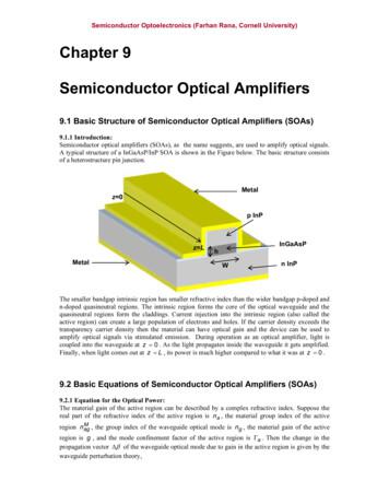
Semiconductor Optical Amplifiers 9.1 Basic Structure of Semiconductor Optical Amplifiers (SOAs) 9.1.1 Introduction: Semiconductor optical amplifiers (SOAs), as the name suggests, are used to amplify optical signals. A typical structure of a InGaAsP/InP SOA is shown in the Figure below. The basic structure consists of a heterostructure pin junction.File Size: 1MB
AWJM, the abrasive particles are allowed to entrain in water jet to form abrasive water jet with significant velocity of 800 m/s. Such high velocity abrasive jet can machine almost any material. Fig. 1 shows the photographic view of a commercial CNC water jet machining system along with close-up view of the cutting head.


