Introduction To CMOS VLSI Design
Introduction toCMOS VLSIDesignCircuits Lecture APeter KoggeUniversity of Notre DameFall 2015, 2018Based on material fromProf. Jay Brockman, Joseph Nahas: University of Notre DameProf. David Harris, Harvey Mudd lOutline: Circuits Lecture A– Physics 101– Semiconductors for Dummies– CMOS Transistors for logic designers Lecture B–––––NMOS LogicCMOS Inverter and NAND Gate OperationCMOS Gate DesignAddersMultipliers Lecture C––––––Pass arrel ShiftersCircuits-ACMOS VLSI DesignSlide 21
EE101 Charge (Q): # of excess electrons beyond # of protons– Units of Coulombs: 1 coulomb 6.24151 1018 electrons Voltage (V): electrical potential difference between two pointin space– Point with lower potential called negative– Point with higher potential called positive Current (I): flow of electrons across a voltage potential– Electrons travel from negative to positive– Units of Amperes (A), where 1 A 1 coulomb moving in 1 sec Resistance (R): property of material controlling amount ofcurrent: I V/R or R V/O or V IR Capacitance (C): property of material to store a charge &form a voltage potential– V Q/C potential when Q charge is stored in a capacitance C– Units of capacitance are Farads,– where 1 volt 1 Coulomb / 1 FaradCircuits-ACMOS VLSI DesignSlide 3Underlying Physics 101 Atoms constructed from– Protons: positively charged heavy particles– Neutrons: heavy particles with no charge– Electrons: very light negatively charged particles Protons & neutrons bind together in nucleusIn neutral atom, # protons # electrons Electrons circle nucleus in orbitals– Ion: numbers not equal; atom is chargedMax electronsin subshellsShell s p d f g TotalK22L2 68M 2 6 1018N2 6 10 1432O2 6 10 14 18 50– Energy of orbital higher the further from nucleus– Higher energy makes it easier to escape– Up to 2 electrons per orbital Orbitals group into shells (K, L, M, N, O, )– # electrons in shell n 2n2– Electrons fill lower shells first Each shell consists of subshells s, p, d, f, – Different subshells have slightly different energiesCircuits-ACMOS VLSI DesignorbitalshellsSlide 42
Periodic Table of Elementsregion of interest for semiconductorsKPeriod: # of shellsLMAtomic #:# of protons#Same color is same “group” – elements with similar propertiesCircuits-ACMOS VLSI DesignSlide 5Electronic Band Structure Valence Shell: outermost shell with electrons Covalent bonds: Atoms near each other with incompletevalence shell “share” electrons that fill valence shell Shells “above” valence shell– Have higher energies– Allow electrons to escape much easier In solids, differences between energy levels in neighboringorbitals becomes small (but non 0), and group into BANDS– Conduction Bands: Those above valence– If conduction band overlaps valence band – electrons can move I.E. “Current” can flow easilyCircuits-ACMOS VLSI DesignSlide 63
Metals and Insulators---- -Na Cl- - MetalMetal: typically valence shell only partially filled may readily lose electrons from valence atoms become positively charged “holes” surrounded by “sea of free electrons”Circuits-ANon-MetalInsulator (non-metal): valence shell is near full tough to pry out an electron when near a metal, loses anelectron to form strong ionic bondCMOS VLSI DesignSlide 7Some MaterialsElementSymbolAtomic rmaniumGe32N428Circuits-ACMOS VLSI DesignElectrons Electronsinto fillValencevalenceSlide 84
What Makes Electrons Move? Coulomb’s Law: Force between two separated charged particles– Force -qiqj/(4πεr2) qi, qj: charges of two particles in coulombs r: distance between charges ε (“episilon”): permittivity of material– If signs of q the same, force is repulsive– If signs different, force is attractive Mass of electron 1/1836’th of proton Electric field around charge i at radius r: E qi/(4πεr2)– In units of Volts: “force per unit charge”– Force on particle j is thus Eqj Electric field between 2 parallel plates with equal & oppositecharges V/dE V/dV Q/CE Q/CdCircuits-ACMOS VLSI DesignSlide 9ResistanceCurrent FlowElectron Flow LVoltage Potential1.2.3.4.5.Conduction electrons drawn from region nearest This leaves positive “holes”Which attract electrons from next region At “-” end, electrons are drawn from potentialCurrent flow is hole flow from into materialand out towards negative end. (OPPOSITE electrons)How much flow depends on Voltage and ResistanceCurrent Voltage / Resistance or Resistance Voltage / CurrentResistance in units of ohms (Ω), or 1Ω 1 Volt / 1 AmpResistance R ρ L / A: A Cross section area L Length of material ρ (rho) Resistivity of material (in units of ohm meter)Circuits-ACMOS VLSI DesignMaterialResistivity, ρ (ohm-meter)Metals10–8Semiconductors variable10 s 0 (exactly)Slide 105
Kirchhoff’s LawsResistance R ρ L / A: A cross section area L length of material ρ resistivity of material (in units of ohm meter)R1R2R R1 R2Why?R1R 1/ (1/R1 1/R2) (R1 R2)/(R1*R2)R2Circuits-AWhy?CMOS VLSI DesignSlide 11Current Density (J)Area ACurrent Density J Current/Area Amps/m2 V/(ρL)(J is a “vector” with direction along path of electrons)Why do we care? Too high a current density can cause: Metal migration Burnout Skin effectCircuits-ACMOS VLSI DesignSlide 126
CapacitorsxBasic device: 2 conducting plates (of area A) Separated by a distance d With “dielectric” insulatormaterial between SiO2 typical on chipsC (in units of Farads F: Coulombs / Volts) ε A / dwhere ε “permittivity” of material, often written as εrε0 ε0 permittivity of vacuum 8.854x10⁻¹² F m-1 εr permittivity of material relative to vacuum 1 F 1 Coulomb / 1 VoltWhat happens with large εr?Circuits-ACMOS VLSI DesignMaterialEpisilon[r]Aluminium‐1.30E 17Silver‐8.50E 25Polyimide3.4Paper3.5Electroactive polymers2–12Silicon dioxide3.9Concrete4.5Pyrex icon11.68Water88Titanium dioxide86–173Strontium titanate310Barium strontium titanate500Barium Slide 13Capacitors in Action(1)(a) Both plates have no chargeWhich Direction isCurrent Flow?Circuits-A(5)(b) Switch closes1. Electrons attracted off of left plate into battery2. Left plate becomes positively charged3. Atoms in dielectric have electrons attracted to left4. This pushes positive charge to right5. Electrons on right plate attracted to leftmost side6. Leaving positive charge in right wire7. Which is neutralized by electrons from – battery8. Current stops when charge Q CVCMOS VLSI DesignSlide 147
Capacitor CircuitsC εA/dC1C2C 1/ (1/C1 1/C2) (C1*C2)/(C1 C2)Why?C1C C1 C2C2Circuits-AWhy?CMOS VLSI DesignSlide 15RC CircuitsVRVRCVCRC “time 2930What does a negativecurrent flow mean?What do we know?1. IR IC I2. V VC VR or VR V-VC3. IR I VR / RIR 4. I I C dV /dtCCorVC V - RC dVC/dtICorVC V(1 – e-t/RC)t/RCCircuits-ACMOS VLSI DesignSlide 168
SemiconductorsCMOS VLSI DesignKey Materials: Si, B, PMaterialAtomic #Electrons per ShellSilicon Si142, 8, 4Boron B52,Phosphorus152, 8, 5Circuits-A3CMOS VLSI DesignSlide 189
SiliconSi: silicon – has 4 electrons and space for 4 more in valence shell- --Si- --Si-Si-free electron- -SiSihole- -- -- -- -- -Si-- -- Si- - Si- - Si- -- -Si-- -- Si - Sifree electronholeT 0o Kthermal excitationT 0o KCircuits-ACMOS VLSI DesignSlide 19Doping: Mixing Into Pure SiliconP or Phosphorus one more electron in valence than Si known as a donor atom- -free electron- P - - - Si- - Si- -B or Boron one less electron in valence than Si known as a acceptor atom- -- --Si- - P - - - Si- ---- free hole-N-typeCircuits-AB-- --SiSi- --- -- -SiB-- --Si-- -P-typeCMOS VLSI DesignSlide 2010
PN Junctions A junction between p-type and n-type semiconductorforms a diode. Current flows only in one directionFree electronsp-typen-typeanodecathodeCurrentFree holesVTVoltageVCircuits-ACMOS VLSI DesignSlide 21The “Why” of PN JunctionsP-- B --Si- Si- -N- -- - - P - - - - SiB- - - - SiSi- - - --Si-DepletionZone- --Si- -- P - - - Si- -- Electrons move from N to P materials With holes that “move right” Until charge near surface at PN repels more-- -- -- -- - P - - - SiSiB- - - - - - Si - Si - - Si- - - - B- ----Si- -Circuits-A- -Si- - P - - - Si- --- Vbi If V 0, no current flows V reinforces depletion zone If 0 V Vbi V cannot overcome attraction in junction Depletion zone shrinks No current flows If V Vbi Electrons pulled left from P-junction Holes in N-type filled with electrons from V Current flowsCurrentVCMOS VLSI Designsi sReVTtorVoltageSlide 2211
nMOS Transistor Four terminals: gate, source, drain, body Gate – oxide – body stack looks like a capacitor– Gate and body are conductors– SiO2 (oxide) is a very good insulator– Called metal – oxide – semiconductor (MOS) capacitor Even though gate is often not metalSourceGateDrainPolysiliconSiO2Gate0n Sourcen SDrainpBodyDbulk SiBodyCircuits-ACMOS VLSI DesignSlide 23nMOS Operation Body is commonly tied to ground (0 V) When the gate is at a low voltage:– P-type body is at low voltage– Source-body and drain-body diodes are OFF– No current flows, transistor is OFFSourceGateDrainPolysiliconSiO2Gate 00n n Spbulk SiBodyCircuits-ACMOS VLSI DesignDSourceDrainBody 0Slide 2412
nMOS Operation Cont. When the gate is at a high voltage:Positive charge on gate of MOS capacitorNegative charge attracted to bodyInverts a channel under gate to n-typeNow electrons can flow through n-type silicon from source throughchannel to drain– Current flows from the drain to the source (Why?)SourceGateDrain– The transistor is ON–––– PolysiliconSiO21n n SpDbulk SiBodyCircuits-ACMOS VLSI DesignSlide 25pMOS Transistor Similar, but doping and voltages reversed–––––Body tied to high voltage (VDD)Gate low: transistor ONGate high: transistor OFF“Bubble” on gate symbol indicates inverted behaviorHoles (and current) flow from the source to the drainSourceGateDrainPolysiliconSiO2Gatep SourceDrainBody 1Circuits-Ap nbulk SiVddCMOS VLSI DesignSlide 2613
Circuit SymbolsNMOSPMOSDrainSourceGateCurrentGateSource CurrentDrainWhen not shown, standard is:– NMOS Body is tied to VSS, the logic negative voltage supply.– PMOS Body is tied to VDD, the logic positive voltage supply.Circuits-ACMOS VLSI DesignSlide 27Key Transistor NLength “Threshold Voltage” on gate that causes current to flow“Resistance” of channel that conducts current“Capacitance” of GateKey Controlling Physical Parameters– Length (L) of channel– Width (W) of Channel– Thickness (tox)of gate insulatorCircuits-ACMOS VLSI DesignSlide 2814
What is Your thWhat Happens as We Make the Following hreshold VoltageCircuits-ACMOS VLSI DesignSlide 29The “Water” Analog Think of electrons as “drops of water” Water flows from high pressure (high voltage) to lowpressure (low voltage) Flow of water can fill up a container (capacitor)– “Height” of water voltage How high a certain amount of water fills a containerdepends on area of container– Wider area higher capacitance more water flow neededto raise level Transistors like toilet “flapper valves”– Turn “on” when water level reaches threshold– Assume threshold 0.5 height in followingCircuits-ACMOS VLSI DesignSlide 3015
CMOS Switching CircuitsA Simple Inverter Computing machines builtPMOSfrom switches Encoding: voltage atVin 0points in circuit Operation: moving chargearoundVddVout MOSNMOS conducts when charge (water)level is above switching thresholdswitchingthresholdPMOS conducts when level belowNo conduction after output container is fullCircuits-ACMOS VLSI DesignSlide 31Signal Propagation (1)t 0Vin 0Vout 0t 0Vin 1Vout 0Circuits-ACMOS VLSI DesignSlide 3216
Signal Propagation (2)t 1Vin 1Vout 0t 2Vin 1Vout 1Circuits-ACMOS VLSI DesignSlide 33Delay and Energy Definitions Propagation Delay– time to fill output container to 50%– time to charge output capacitance to 50% Switching Energy– weight x height of water moved– charge x voltage of charge transferred– QxV CVxV CV2Circuits-ACMOS VLSI DesignSlide 3417
Circuits-A CMOS VLSI Design Slide 2 Outline: Circuits Lecture A – Physics 101 – Semiconductors for Dummies – CMOS Transistors for logic designers Lecture B – NMOS Logic – CMOS Inverter and NAND Gate Operation – CMOS Gate Design – Adders – Multipliers Lecture C – P
CSCE 5730: Digital CMOS VLSI Design 29 IC Categories Functions Analog ICs Amplifiers Filters Digital ICs Boolean Gates Encoders/Decoders Multiplexers / Demultiplexers Flip-flops Counters . Digital IC Design Flow CSCE 5730: Digital CMOS VLSI Design 36. Technology Growth and Moore's Law CSCE 5730: Digital CMOS VLSI Design 37.
CMOS VLSI Design A Circuits and Systems Perspective. Fourth Edition Neil H. E. Weste Macquarie University and The University of Adelaide David Money Harris Harvey Mudd College CMOS VLSI Design A Circuits and Systems Perspective Addison-Wesley Boston Columb
Principles of VLSI Design Introduction CMPE 315 Principles of VLSI Design Instructor Chintan Patel (Contact using email: cpatel2@cs.umbc.edu). Text CMOS VLSI Design: A Circuits and Systems Perspective, Third Edition. by Neil H.E. Weste and David Harris. ISBN: 0-321-14901-7, Addison Wesl
VL2114 RF VLSI Design 3 0 0 3 VL2115 High Speed VLSI 3 0 0 3 VL2116 Magneto-electronics 3 0 0 3 VL2117 VLSI interconnects and its design techniques 3 0 0 3 VL2118 Digital HDL Design and Verification 3 0 0 3 VL2119* Computational Aspects of VLSI 3 0 0 3 VL2120* Computational Intelligence 3 0 0 3
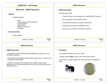
Module #3 CMOS Fabrication Agenda 1. CMOS Fabrication - Yield - Process Steps for MOS transistors - Inverter Example - Design Rules - Passive Components - Packaging Announcements 1. Read Chapter 2 Module #3 ECOM 5335 VLSI Design Page 2 CMOS Fabrication CMOS Fabrication - We have talked about
Rochester Institute of Technology Microelectronic Engineering CMOS VLSI DESIGN Page 8 RIT SUBµ CMOS RIT Subµ CMOS 150 mm wafers Nsub 1E15 cm-3 Nn-well 3E16 cm-3 Xj 2.5 µm Np-well 1E16 cm-3 Xj 3.0 µm LOCOS Field Ox 6000 Å Xox 150 Å Lmin 1.0 µm LDD/Side Wall Spacers Vdd 5
VLSI Design 2 Very-large-scale integration (VLSI) is the process of creating an integrated circuit (IC) by combining thousands of transistors into a single chip. VLSI began in the 1970s when complex semiconductor and communication technologies were being developed. The microprocessor is a VLSI device.
Unit-1: Introduction and Classification of algae (04L) i) Prokaryotic and Eukaryotic algae ii) Classification of algae according to F. E. Fritsch (1945), G.W. Prescott and Parker (1982)


