Band Structure And Optical Properties Of Pseudomorphic Ge1 .
Band Structure and Optical Propertiesof Pseudomorphic Ge1-x-ySixSny on GeNalin Fernando,1 Ryan Hickey,2 John Hart,2 Ramsey Hazbun,2Dainan Zhang,2 James Kolodzey2, Stefan Zollner,11Department of Physics, New Mexico State University, Las Cruces, NM2 Department of Electrical and Computer Engineering, University of Delaware, Newark, DEAFOSR: FA9550-13-1-00221
Ge1-ySixSny Alloys for Photonic Devices Ge indirect band gap material. Relaxed Ge1-ySny alloys become direct at 6-9% Sn Ge1-x-ySixSny band structure depends on- Strain- Composition- TemperatureGe1-x-ySixSnyGe substrate Pseudomorphically grown Ge1-x-ySixSny has low defectdensity and no dislocations. By using spectroscopic ellipsometry we can determine the bandgaps by looking at optical properties. Used spectroscopic ellipsometry and HRXRD to characterizestrain and compositional dependence of the optical properties ofpseudomorphic Ge1-ySny (Si 0) on Ge grown by MBE. 2
Pseudomorphic Ge1-x-ySixSny Alloys on GerelaGe1 x ySi x Sn y xaSi yaSn (1 x y )aGe bGeSn y (1 x y ) bGeSi x(1 x y ) bSiSn xyε 0Ge1-x-ySixSnyε 0aSn 6.489 Å,aGe 5.657 Å,aSi 5.453 Åε 0GeIn-plane strain:ε relaGe aGe1 x yrelaGe1 x y C12 C11 Ge1 x y Si x Sn y Out-of-plane strain:ε 2Si x Sn ySi x Sn yGe Si SnC12 1 x y x yGe Si SnC11 1 x y x yGeCmn1 x ySi x Sn yC12 εC11GeSiSn xCmn yCmn (1 x y )CmnKouvetakis et al., Annu. Rev. Mater. Res. 36, 497 (2006)3
Strain and Compositional Dependenceof Band GapsrelEcΓ Edir, Γ 3avε HLL1 LrelEc Eind , L 3 Ξ d Ξ d av ε HEindXStrainedconductionband EcX 4 relEind,XBauer et al., Solid State Commun. 127, 355 (2003)EcX 2ε H Hydrostatic strainε S Shear strainavX1 Ξ d Ξ d av 3 Lb X1 3 Ξ d Ξ d av ε H ε S Ξ d 3 X1 3 Ξ d Ξ d av ε H 2ε S Ξ d3 31 2 0 6 0bε S (9bε S ) 2EvΓ 0 bε S 12 22EvΓ 3bε S21 Ξ d Ξ d av 3 Ξ dStrainedvalenceband relEind,X3 31 2EvΓ 0 bε S 0 6 0bε S (9bε S ) 232 22S. T. Pantelides and S. Zollner, Silicon-Germanium Carbon Aloys Growth, Properties and Applications (Taylor & Francis, NewYork, NY, 2002)Kurdi et al., Appl. Phys. 107, 013710 (2010)Beeler et al., IEEE J. Photovolt. 2, 434 (2012)4
E1 Critical Point Energy ES ( y ) 6 D33ε S E H ( y ) 3D11ε HE1s ( y ) E10 ( y ) E H ( y ) 1 ( y ) 21 ( E1 1 ) ( y ) ( E1 1 ) ( y ) E H ( y ) Es224sBauer et al., Solid State Commun. 127, 355 (2003) 1 ( y ) 21 Es2240V. R. D'Costa et al., J. Appl. Phys. 116, 053520 (2014)4040ε1 Geε1 10% Snε2 Geε2 10% Sn30E1 Δ10-10-200.0E2E110E01.020E0’2.03.04.0Photon Energy (eV)ε2ε12030105.006.05
Pseudomorphic Ge1-x-ySixSny Alloys on GeIn-plane strain ε Band gap at Γ (eV)Band gap at X (eV)Band gap at L (eV)6
Strain and Compositional Dependenceof Band GapsSmallest band gap morphic Ge1-x-ySixSny alloys become direct forSi 13% and Sn 17%.7
Ge1-x-ySixSny Alloys on Ge Buffered SiEffects of the thermal expansion mismatch of the Ge buffer and SiLattice matched Ge1-x-ySixSnyGe1-x-ySixSnyGe bufferGrowth temp. TgSi substrateTgε (T ) [α Ge (T ) α Si (T )] dTT1αν (T ) 3 4Χi 1 i(θi / T )2 exp(θi / T )[exp(θi / T ) 1]2Reeber et al., Mater. Chem. Phys. 46, 259 (1996)Indirect to direct band gap crossover of Ge1-x-ySixSny;On bulk GeOn Ge buffered Si, Tg 770 KOn Ge buffered Si, Tg 1200 K8
Lattice parameter and Strain of Ge1-ySnyAlloys on Ge by MBEnts/s10M1M00K10K1KRSM(224) ge(0 0 4) ω-2θThicknessGesubstrateGeSn layerInterferencefringes100Composition10131.6 31.8 32.0 32.2 32.4 32.6 32.8 33.0Omega/2Theta ( )Hydrostatic strain:Shear strain:εH εS ε 2ε 3ε ε 39
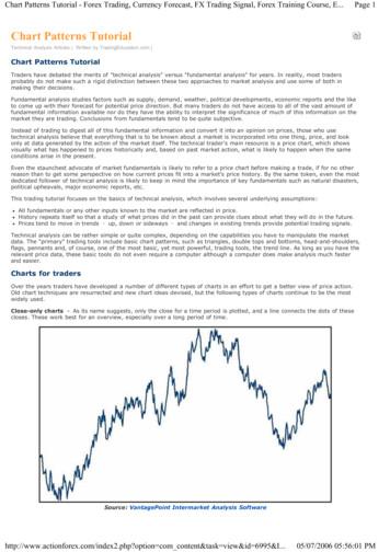
Optical Constants of Ge1-ySny Alloys4025 ε1 Ge ε1 2% Sn ε1 7.3% Sn ε1 11% Sn ε2 Ge ε2 2% Sn ε2 7.3% Sn ε2 11% Sn282117134-8-201.01.92.73.64.45.3Photon Energy (eV)d2ε/dE2 Analysis of CP parameters;E- energy, A- amplitude,Γ- broadening, φ- phase1 Ge1-ySny1046 Å40 Ge1 mmParametric model fit andthen point-by-point fit toobtain the dielectric functionof the alloy.40Real(Dielectric Constant), ε1Viña et al., Phys. Rev. B 30, 1979 (1984)40 Å40ε1 Geε1 2% Snε1 7.3% Snε1 11% Snε2 Geε2 2% Snε2 7.3% SNε2 11% Sn302010E1, E1 Δ13020010-10-201.52.33.03.84.5Photon Energy (eV)5.306.010Imag(Dielectric Constant), ε2ε C A ln(E ω iΓ) eiϕ2 GeO2807.06.1 E1, E1 1: 2D critical points ε2 ε1 16Measured pseudodielectric function
Direct band gap of Ge1-ySny Alloys9.7% Sn20.05.019.04.0Model Fit ε1 at 60 ε1 at 65 ε2 at 60 ε2 at 65 3.0 ε2 ε1 18.0 FTIR ellipsometry 0.1 – 0.7 eV. Poor signal to noise ratio.17.02.016.01.00.20.60.50.40.3Photon Energy (eV)35 E0: 3D critical points30eViña et al., Phys. Rev. B 30, 1979 (1984)2520ε1 Geε1 7.6% Snε1 9.7% Snε1 11% Snε2 Geε2 7.6% Snε2 9.7% Snε2 11% Sn1510ε21/2 iϕε C A (ω E iΓ)0.00.7ε115.00.1Parametric oscillatormodel fit(simultaneously withIR-UV data)20150.050.51.0Photon Energy (eV)1.502.0Decreasing direct band gap (E0) with increasing Sn content.11
Ge band Splitting and Shifting with SnPseudomorphic Ge1-ySny on GeEc(L) always lower than the Ec(Γ). Edirect EindirectPseudomorphic GeSn alloysnever become direct12
Summary Direct and indirect band gaps can be modeled usingdeformational potential theory for pseudomorphic Ge1-x-ySixSnyalloys grown on Ge. Increasing the growth temperature of the Ge buffer layerreduces the compressive strain reduces the x (Si) and y (Sn)for the indirect to direct crossover. Deformation potential theory predicts no indirect to direct bandgap crossover for pseudomorphic (fully strained) Ge1-ySnyalloys on Ge. Theoretical predictions are validated using ellipsometry forpseudomorphic GeSn alloys (Si 0) on Ge.13
Band Structure and Optical Properties of Pseudomorphic Ge 1-x-ySi xSn y on Ge Nalin Fernando,1 Ryan Hickey,2 John Hart, 2 Ramsey Hazbun, Dainan Zhang, 2James Kolodzey , Stefan Zollner, 1 1. Department of Physics, New Mexico State University, Las Cruces, NM
Affairs Group 75: Records of the Osage Agency - Annuity Payment Rolls, 1880-1907 (Roll 1 of 21) Osage Annuity Payment Roll: 1 st and 2nd Quarters of 1880 o Big Chief Band o Joe's Band o Big Hill Band o White Hair Band o Tall Chief Band o Black Dog Band o Saucy Chief Band o Beaver Band o Strike Axe Band o No-Pa-Walla Band
Cope & Stick - 500 Series Veneer Doors Miter Frame - 500 Series. Style Band 1 Band 2 Band 3 Band 4 Band 5 101 Glass 10 12 13 16 18 Material Band 1 Band 2 Band 3 Band 4 Band 5 102/104 Glass 12 14 15 18 20 Paint X Notes - PRICES ARE PER SQ/FT Maple Paint X Minimum Dimensions - Doors 7"W x 7"H Natural Soft Maple X
CEFR level: IELTS band: C1 IELTS band: 8 IELTS band: 7.5 IELTS band: 7 B2 IELTS band: 6.5 IELTS band: 6 IELTS band: 5.5 IELTS : 4.5 IELTS band: 4 IELTS band: 5 978-X-XXX-XXXXX-X Author Title C M Cullen, French and Jakeman Y K Pantoene XXX STUDENT'S BOOK with DVD-ROM WITH ANSWERS B1-C1 The
WIKUS BAND SAW BLADES Bimetal band saw blades Diamond coated band saw blades Carbide band saw blades Carbon steel band saw blades Sales units: coils in fixed lengths and manufacturing coils up to 120 m, depending on the band width, welded-to-length band saw blades Band widths: 4 to 125 mm Constant tooth pitches: 0,75 to 18 teeth per inch (tpi)
Semiconductor Optical Amplifiers (SOAs) have mainly found application in optical telecommunication networks for optical signal regeneration, wavelength switching or wavelength conversion. The objective of this paper is to report the use of semiconductor optical amplifiers for optical sensing taking into account their optical bistable properties .
Mar 20, 2006 · B-BAND A3T SIDEMOUNT PREAMP WITH B-BAND UST OR AST TRANSDUCER This is a basic installation manual and tip sheet. For more information, technical support, and pictures of installations about all B-Band products please check the B-Band website at www.b-band.com or contact your B-Band dealer, distributor or B-Band directly. Date: 5th May 2007 .File Size: 435KBPage Count: 16
TD-HSDPA/HSUPA: 2.8Mbps DL, 2.2Mbps UL EDGE: Multi Slot Class 12 236.8 kbps DL & UL GPRS: Multi Slot Class 10 85.6 kbps DL & UL Frequency Bands: LTE Band B1 (2100MHz) LTE Band B2 (1900MHz) LTE Band B3 (1800MHz) LTE Band B4 - AWS (1700MHz), LTE Band B5 (850MHz), LTE Band B7 (2600MHz) LTE Band B8 (900MHz) LTE Band B12 (700MHz) LTE
A novel all-optical sampling method based on nonlinear polarization rotation in a semiconductor optical amplifier is proposed. An analog optical signal and an optical clock pulses train are injected into semiconductor optical amplifier simultaneously, and the power of the analog light modulates the intensity of the output optical pulse through


