Experiments #4 Frequency Response Of BJT
Electronics II LabEELE 3120Experiments #4Frequency Response of BJT1) Objectives:To study the frequency response and bandwidth of the common emitter CE-BJT, thecommon collector CC-BJT, and the common base CB-BJT amplifiers.2) Introduction:Most amplifiers have relatively constant gain across a range or band of frequencies, thisband of frequencies is referred to as the bandwidth (BW) of the circuit.Bandwidth means the difference between the upper and lower frequencies of thefrequency response as shown in the figure 4.1Figure 4.1: the frequency response of BJTWhen operated within its bandwidth, the values of 𝐴𝑣 & 𝐴𝑖 for an amplifier are calculatedas shown earlier, these values are referred to as mid-band gain values, and aredesignated as 𝐴𝑣𝑚𝑖𝑑 & 𝐴𝑖𝑚𝑖𝑑 .The frequency response is a graphical representation of the relationship betweenamplifier gain and operating frequency for input signal, as an example sinusoidal signal.Page 1 of 8
Electronics II LabEELE 3120So why we need this type of analysis for an amplifier, because we need to determine the:-To determine the stability region for amplifier systems.To design an amplifier systems that met the required specifications.3) AC & DC Analysis:a) DC Analysis:As we know the frequency in DC is equal zero because there is no oscillation in DCsignal so, the reactance of capacitor is equal infinity that mean the capacitors work asopen circuit.b) AC Analysis:In this analysis we will study the effect of capacitors in different level of frequenciesas: Low frequencyMiddle frequencyHigh frequencyBefore we start our analysis we need first know the names of capacitors and itslocations, there are two type of capacitor: Practical capacitors: Cin, Cout, CE these capacitors are connected as shown infigure 4.1 and it’s effective in low frequency.Virtual capacitors: Cwi, Cwo, CBE, CBC, CCE these capacitors are appears andeffectives on the high frequency because its value in Nano-farad.Page 2 of 8
Electronics II LabEELE 3120Cases of capacitor: At very low frequency the capacitor work as open circuit.At very high frequency the capacitor work as short circuit.At normal frequency the capacitor have a magnitude and effect on thefrequency response.𝑋𝑐 12𝜋𝑓𝑐Now, we will show the relationship between the voltage gain and varying frequencyand defined the regions on this curve as shown in figure 4.2Figure 4.2: The frequency response of BJT amplifierFigure 4.3: The sample circuit diagram of BJT amplifierPage 3 of 8
Electronics II Lab EELE 3120Low frequency response of BJT amplifier: (𝟎 𝑭𝒍𝒐𝒘 )At this region all capacitors will be open circuit because its reactance will beequal infinity at 𝑓 0 and 𝐴𝑣 0.Now, if the frequency increase slightly the voltage gain will be increase also untilthe frequency reach to low cut frequency, after this critical point the capacitorswill be short circuit and voltage gain raise to the maximum value (𝐴𝑣(𝑚𝑖𝑑) ).1- 𝐶𝑖𝑛 𝑎𝑡 𝐶𝑜𝑢𝑡 & 𝐶𝐸 short circuit:𝑓𝑙𝐶𝑖𝑛 12𝜋(𝑅𝑠 𝑍𝑖)𝐶𝑖𝑛Where: 𝑍𝑖𝑛 𝑅1//𝑅2//𝐵𝑟𝑒2- 𝐶𝑜𝑢𝑡 𝑎𝑡 𝐶𝑖𝑛 & 𝐶𝐸 short circuit:𝑓𝑙𝐶𝑜𝑢𝑡 12𝜋(𝑅𝑜 𝑅𝑙)𝐶𝑜𝑢𝑡3- 𝐶𝐸 𝑎𝑡 𝐶𝑖𝑛 & 𝐶𝑜𝑢𝑡 short circuit:𝑓𝑙𝐶𝐸 1𝑅 𝑠 𝐵𝑟𝑒2𝜋 (𝑅𝐸 ) 𝐶𝐸𝐵Where: 𝑅 𝑠 𝑅𝑠//𝑅1//𝑅2 High frequency response of BJT amplifier: (𝑭𝒉𝒊𝒈𝒉 )In this region will be appear the effect of virtual capacitors which called parasiticeffect (𝐶𝑤𝑖, 𝐶𝑤𝑜, 𝐶𝐵𝐸, 𝐶𝐶𝐸, 𝐶𝐶𝐵), and its value in Nano-farad.These capacitors at very high frequency will be short circuit and it reactance equalzero, and the voltage gain goes to zero.In this region all practical capacitors are short circuit also.Page 4 of 8
Electronics II LabEELE 31201- At 𝐶𝑖𝑛, 𝐶𝑜𝑢𝑡, 𝐶𝐸 are shortcircuit:𝐶𝑖 �� 𝐶𝐵𝐸[1 𝐴𝑣]𝐶𝑖 𝐶𝑤𝑖 𝐶𝐵𝐸 𝐶𝑚𝑖𝐶𝑜 �� 𝐶𝐵𝐶[1 1]𝐴𝑣𝐶𝑜 𝐶𝑤𝑜 𝐶𝐶𝐸 𝐶𝑚𝑜2- High frequency law:𝑓ℎ𝑖 12𝜋𝑅𝑡ℎ𝑖 𝐶𝑖𝑓ℎ𝑜 12𝜋𝑅𝑡ℎ𝑜 𝐶𝑜𝑅𝑡ℎ𝑖 � 𝑅𝐿//𝑅𝑐//𝑟𝑜Page 5 of 8
Electronics II LabEELE 3120Before we are going to lab work we need to know some important definitionswhich we need them in design.Logarithm:𝑥 log 𝑏 𝑎 , 𝑎 𝑏 𝑥Why we need log scale? To represent a large scale of frequency start from 𝐻𝑧 andgoes to 𝑀𝐻𝑧.There are two modes of log scale:-Semi Log: that mean the x-axis is logarithm increment and y-axis is linearincrement.Double Log: that mean the x-axis and y-axis are logarithm increment.Decibels: (dB)1 𝑑𝐵 10 log10𝑝2𝑝11 𝑑𝐵 20 log10 𝐴𝑣Notes:-To find the Low cut off frequency 𝑓𝐿 𝑀𝐴𝑋(𝑓𝐿𝑐𝑖𝑛 , 𝑓𝐿𝑐𝑜𝑢𝑡 , 𝑓𝐿𝑐𝑒 ).To find the upper cut off frequency 𝑓𝐻 𝑀𝐼𝑁(𝑓𝐻𝑖 , 𝑓𝐻𝑜 )Page 6 of 8
Electronics II LabEELE 31204) Lab work:Figure 4.4: Common Emitter Amplifier1- Connect the circuit in figure 4.4.2- Adjust the DC power supply at 20Vdc.3- Adjust the function generator to sinusoidal of 𝑉𝑝 1𝑉𝑎𝑐 at a frequency 1𝐾𝐻𝑧.4- Measure the output voltage Vo RMS value (AC mode in Multi-meter device).5- Calculate 𝐴𝑣𝑚𝑖𝑑 & 0.707𝐴𝑣𝑚𝑖𝑑 which be equal 0.707𝑉𝑜 because the input voltageequal 1𝑉𝑎𝑐.6- Now decrease the frequency of input signal to get 𝑉 𝑜 0.707𝑉𝑜 on Multi-meterscreen to find 𝑓𝐿 .7- Then increase the frequency of input signal to get 𝑉 𝑜 0.707𝑉𝑜 on Multi-meterscreen to find 𝑓𝐻 .8- Now calculate the Bandwidth 𝐵𝑊 𝑓𝐻 𝑓𝐿 .9- Now varying the frequency of function generator according to table 1 shown belowand measure the variable on each level.10- Plot the voltage gain 𝐴𝑣 relative to frequency.Page 7 of 8
Electronics II LabEELE 3120Frequency (Hz)Vin (RMS)Vo (RMS)𝑨𝒗 𝑽𝒐 𝑽𝒊𝒏1101001k10k50k100k1M2M5MTable 1: Common Emitter Amplifier result5) Exercise:1- Repeat all steps for common emitter amplifier using Orcad.2- Repeat all steps for emitter follower amplifier which shown below using Orcad.Page 8 of 8
Frequency Response of BJT 1) Objectives: To study the frequency response and bandwidth of the common emitter CE-BJT, the common collector CC-BJT, and the common base CB-BJT amplifiers. 2) Introduction: Most amplifiers have relatively
Thursday, March 24, 2016 - Friday, March 25, 2016 4. The New Frequency Response Obligation 4.1. Frequency Response Standard The new frequency response standard will require each BA to achieve a Frequency Response Measure (FRM) that meets its FRO starting in the 2017 compliance period (i.e. December 2016 through November 2017).
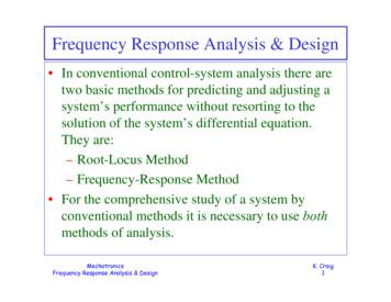
response is easily obtained by means of the inverse Laplace Transform. Frequency-Response Method – Frequency response is the steady-state response of a system to a sinusoidal input. In frequency-response methods, we vary the frequency of the input signal over a certain
the 2012 Frequency Response Initiative Report because the actual frequency nadir was accurately captured. The frequency response analysis tool11 is being used by the NERC Bulk Power System Awareness group for frequency event tracking in supp
High-Frequency Response of CS Amp Take the following circuit and investigate its high-frequency response – First, redraw using a high-frequency small-signal model for the nMOS There are two ways to find the upper 3-dB frequency ω H – Use open-circuit time constant method
The simulation model in this circuit is designed for frequency response, and the functions not related to frequency response are not implemented. Table 4. BD9E200FP4_AC model pins used for frequency response Pin Name Description VIN Power supply input. EN Enable input. BOOT Pin for bootstrap. SW Switching node. FB Output voltage feedback pin.
College London (UCL) to investigate the potential uses of experiments in understanding consumer behaviour, and to develop a better understanding of the potential benefits of experiments if used in Ofcom's work. 1.2 The potential uses of experiments . Experiments test the actual behaviour of individuals under different conditions. In an
treatment e ects, and propose a novel experimental design in this setting. Our paper adds to both the literature on single-wave and multiple-wave experiments. In the context of single-wave (or two-wave) experiments, existing network experiments include clustered experiments (Eckles et al.,2017;Ugander et al.,2013;Karrer et al.,2021) and satu-
4 Sensor Experiments 4.1 Search & Rescue Experiments Experiments were conducted on February 11, 2005 at the Lakehurst Naval Air Base, NJ as part of the New Jersey Task Force 1 search and rescue train-ing exercise. The purpose of the experiments was to validate the utility of sensor networks for mapping, to characterize the ambient conditions of .


