High Speed Analog To Digital Converter Basics
Application ReportSLAA510 – January 2011High-Speed, Analog-to-Digital Converter BasicsChris Pearson.ABSTRACTThe goal of this document is to introduce a wide range of theories and topics that are relevant tohigh-speed, analog-to-digital converters (ADC). This document provides details on sampling theory,data-sheet specifications, ADC selection criteria and evaluation methods, clock jitter, and other commonsystem-level concerns. In addition, some end-users will want to extend the performance capabilities ofADCs by implementing interleaving, averaging, or dithering techniques. The benefits and concerns ofinterleaving, averaging, and dithering ADCs are discussed in this document.1234567ContentsIntroduction . 2Spectral Performance Terminology . 4Nyquist, Aliasing, Undersampling, Oversampling, and Bandwidth . 4Interfacing With ADC Pins . 84.1Analog Inputs . 84.2Reference/Common Mode . 104.3Clock Inputs/Jitter . 114.4Laboratory Evaluation . 15Advanced Topic 1: Interleaving ADCs . 18Advanced Topic 2: Averaging ADCs . 21Advanced Topic 3: Dithering . 23List of Figures1234567891011121314151617181920. 2Frequency Domain vs Time Domain . 3ADC Performance Terminology . 4Oversampling Fin Fs/2 . 5Undersampling Fin Fs/2 . 5Oversampling and Undersampling in Both Time and Frequency Domains . 6Desired and Undesired Aliasing . 7Analog Input Bandwidth . 8Differential Input Characteristics . 9Differential vs Single-Ended Signal Swing. 9Using Transformers to Drive an ADC Input . 10Effects of Jitter on SNR and ENOB . 11Time Domain Clock Jitter Effects on High- and Low-Frequency Analog Input . 12ADC Aperture Jitter From Data Sheet . 13Clock Slope, Aperture Jitter . 14Sine Wave Clock Amplitude vs SNR . 15FFT Window and Spectral Leakage . 16Rule 3 – Mutually Prime . 17Typical ADC Laboratory Setup . 18Interleaving ADC Example . 19Basic ADC Diagram and TerminologySLAA510 – January 2011Submit Documentation FeedbackHigh-Speed, Analog-to-Digital Converter BasicsCopyright 2011, Texas Instruments Incorporated1
Introduction21222324252627www.ti.com.Interleaved ADC Spectral Plots .Averaging Two ADCs Example .Averaging Two ADCs Benefits .SNR Averaging Improvement vs Number of ADCs .Dithering Diagram .Example of Affects of Dithering .Interleaving Benefits19212222232424List of Tables11Interleaved ADC Error Spectral Locations . 20IntroductionAnalog-to-digital converters (ADC) are devices that sample continuous analog signals and convert theminto digital words. ADCs comprise many categories among which are sigma-delta ADCs, high-resolutionADCs, and high-speed ADCs. This application report focuses on high-speed ADCs.Figure 1 provides the basic block diagram, functionality, and common terminology for ADCs. This figureshows an analog signal applied to the input of the ADC, which then is converted to digital words at thesampling frequency (Fs) applied to the ADC clock. Figure 1 is a time domain representation of the ADC’sinput and output signals.Analog Input:Frequency (Fin)Digital OutputVolts(V)6-BitADCTime D5 D41/Fs0 12/Fs1 03/Fs1 1.N-2/Fs 0 1N-1/Fs 0 0N/Fs1 gFrequency(Fs)Time (s)t1D5D4D3D2D1D0t2Fin: Analog Input Frequency 1/(t2 - t1)Fs: Clock FrequencyN: number of digital samples capturedn: number of output bits; in this 6-bit ADC example n 6Figure 1. Basic ADC Diagram and TerminologyTime domain representations often are described as real-world signals. In Figure 1, notice that the analoginput’s amplitude is shown in volts (linear) and seconds (linear). Also notice that the digital output codesare listed with time stamps (1/Fs, 2/Fs, 3/Fs ). Time domain representations are often easy to visualize,and they help with understanding gross concepts. However, time domain representations do aninadequate job of measuring the performance of ADCs and other signal-processing devices. Measuringperformance is best accomplished in the frequency domain. Therefore, it is important to understand howthe time domain and frequency domain relate.2High-Speed, Analog-to-Digital Converter BasicsCopyright 2011, Texas Instruments IncorporatedSLAA510 – January 2011Submit Documentation Feedback
Introductionwww.ti.comAnalog Input - Time DomainFrequency (Fin)Digital 0100.111Clock:SamplingFrequency(Fs)Time (s)t1Time D5 D41/Fs0 12/Fs1 03/Fs1 1.N-2/Fs 0 1N-1/Fs 0 0N/Fs1 1D5D4D3D2D1D0t2Analog Input - Frequency DomainFrequency FinDigital Output - Frequency DomainFrequency FinFinFinPower(dBm)Power(dBm)Harmonics, Fin integer234Harmonics 3, 4 & 5have aliased4 553 2Noise FloorFrequency (Hz)Frequency (Hz)FsFs/2 - NyquistFin: Analog Input Frequency 1/(t2 - t1)Harmonics: integer multiples of Fin (2 Fin, 3 Fin, 4 Fin, 5 Fin )Fs: Clock FrequencyNyquist: Fs/2Aliasing: the placement of frequencies Fs/2 (Nyquist) in the Digital OutputFrequency Domain, explained later in more detailFigure 2. Frequency Domain vs Time DomainFigure 2 demonstrates a high-level overview of the differences between the time domain and thefrequency domain. Frequency domain plots are measured in signal power (log scale) and frequency(linear). In the Figure 2 frequency domain plots, the signal imperfections are labeled as noise andharmonics. Notice the ease with which one can identify and quantify these imperfections. Frequencydomain plots also are commonly termed spectrums, spectral plots, or Fast Fourier Transforms (FFT). InFigure 2, the terms Nyquist, harmonics, and aliasing are introduced. These important signal-processingterms are discussed later in more detail.SLAA510 – January 2011Submit Documentation FeedbackHigh-Speed, Analog-to-Digital Converter BasicsCopyright 2011, Texas Instruments Incorporated3
Spectral Performance Terminology2www.ti.comSpectral Performance TerminologySNR: signal-to-noise ratio. SNR is the ratio of the fundamental (PS) to the noise floor (PN), excluding thepower at DC and in the first five harmonics. The first five harmonics are labeled 2 to 6 in Figure 3. Thefundamental is technically the first harmonic, but is rarely called a harmonic. Some data sheets mayexclude the first nine harmonics. Other names for the fundamental tone are signal or carrier. SNR is eithergiven in units of dBc (dB to carrier) when the absolute power of the fundamental is used as the reference,or dBFS (dB to full scale) when the power of the fundamental is extrapolated to the converter full-scalerange. See Figure 3 for the SNR equation and illustration.SFDR: spurious free dynamic range. SFDR is the ratio of the power of the fundamental (PS) to the nexthighest spur (PH). See Figure 3 for the SFDR equation and illustration.THD: total harmonic distortion. THD is the ratio of the power of the fundamental (PS) to the power of thefirst five harmonics (PD). THD is typically given in units of dBc (dB to carrier). See Figure 3 for the THDequation and illustration. Like SNR, some data sheets may use the first nine harmonics for THD.SINAD: signal noise and distortion. SINAD is the ratio of the power of the fundamental (PS) to the powerof all the other spectral components including (PN) and distortion (PD), but excluding dc. SINAD is eithergiven in units of dBc (dB to carrier) when the absolute power of the fundamental is used as the reference,or dBFS (dB to full scale) Figure 3when the power of the fundamental is extrapolated to the converterfull-scale range. See Figure 3 for the SINAD equation and illustration.ENOB: effective number of bits. ENOB is a measure in units of bits of converter performance ascompared to the theoretical ideal SNR limit based on quantization noise (Equation 1). See for the ENOBequation.SNR 10log10 (PS/PN)SFDR 10log10 (PS/PH)THD 10 log10 (PS/PD)SINAD 10log10 PS/(PD PN)ENOB (SINAD - 1.76)/6.02Digital Output - Frequency DomainFrequency FinFinPower(dB)PS: Signal Power (red)PN: Noise Floor Power (blue)PD: Power of harmonics 2-6 (black)PH: Power of next highest spur (black)Fundamental652 43Frequency (Hz)Fs/2In this plotharmonic #3would be PH in theSFDR calculation,since it is thelargest nonfundamental spur.Figure 3. ADC Performance TerminologyIdeal SNR: For a specific converter the ideal SNR can be calculated as shown in Equation 1. Thisequation is mathematically equivalent to the ENOB calculation, where n ENOB and Ideal SNR SNR.Also of importance is that for an ideal converter there is no harmonic content, therefore SINAD SNR.Ideal SNR 6.02 n 1.76n number of bits(1)As an example, a designer may ask for an ADC with 75-dB SINAD. Using Equation 1,one may assumethat the designer requires a 14- or 16-bit ADC (e.g., ENOB (75 dB – 1.76)/6.02 12.2 bits). Otherconsiderations like ADC clock speed, SFDR, bandwidth, and current consumption can further narrowdown which 14- or 16-bit ADC the designer requires. These considerations are discussed further.3Nyquist, Aliasing, Undersampling, Oversampling, and BandwidthThe terms Nyquist, aliasing, undersampling, and oversampling are basic ADC terms. They are all closelyrelated, and sometimes this close relationship causes confusion. Once understood, however, the conceptsare fairly simple.The Nyquist-Shannon sampling theorem states that for a true representation of waveform X, greater than4High-Speed, Analog-to-Digital Converter BasicsCopyright 2011, Texas Instruments IncorporatedSLAA510 – January 2011Submit Documentation Feedback
www.ti.comNyquist, Aliasing, Undersampling, Oversampling, and Bandwidthtwo samples per period are required. For an ADC, this means for a true representation of the analog inputsignal, the clock frequency (Fs) must be two times greater than the analog input frequency (Fin). To statethe last sentence in equation form, when Fin Fs/2, then Fin can be accurately represented. Fs/2 iscommonly referred to as the Nyquist Frequency. Figure 4 and Figure 5 illustrate this theorem graphically.In Figure 4, with Fin Nyquist, notice that the ADC-captured output properly represents the analog input.Analog Input Frequency NyquistAnalog InputADC captureFigure 4. Oversampling Fin Fs/2Figure 4 is also an example of ADC oversampling, as more than two samples are captured per the analoginputs period. To state the last sentence in equation form, when Fin Fs/2, the ADC is oversampling theinput waveform.In Figure 5, with Fin Nyquist, the ADC capture output has translated the analog input signal at a lowerfrequency. This frequency translation is called aliasing. As seen in Figure 5, aliasing happens when Fin Nyquist.Analog Input Frequency NyquistAnalog InputADC captureFigure 5. Undersampling Fin Fs/2SLAA510 – January 2011Submit Documentation FeedbackHigh-Speed, Analog-to-Digital Converter BasicsCopyright 2011, Texas Instruments Incorporated5
Nyquist, Aliasing, Undersampling, Oversampling, and Bandwidthwww.ti.comFigure 5 is an example of ADC undersampling (Nyquist Fin), as less than two samples are captured perperiod. To state the last sentence in equation form, when Fin Fs/2, the ADC is undersampling the inputwaveform. Undersampling allows for an aliased representation of the waveform to be captured.Compare the ADC capture waveforms in Figure 4 and Figure 5 to understand the effects of the Nyquistfrequency (Fs/2), aliasing, oversampling, and undersampling in the time domain. Figure 6 uses the timedomain plots in Figure 4 and Figure 5 to describe aliasing, oversampling, and undersampling in thefrequency domain.ADC OversamplingADC output SpectrumAnalog Input Frequency NyquistFso/8Fso/4 3 Fso/8 Fso/2ADC UndersamplingADC output SpectrumAnalog Input Frequency NyquistFsu ¼ FsoAliasingFsu/2Compare Oversampling to Undersampling:In the ADC Oversampling time and frequencydomain plots the ADC output correctly representsFin.In the ADC Undersampling time and frequencydomain plots the ADC output Fin resembles a lowerfrequency (aliased frequency).Figure 6. Oversampling and Undersampling in Both Time and Frequency DomainsAt first, aliasing may appear to be undesirable. However, it can be very useful. The most useful property ismixing a higher frequency signal to a lower frequency signal. For the system designer, this can translateinto cost savings, power savings, or board-space savings by removing the need for an additional mixer ina designer’s schematic. To achieve these desirable savings, care must be taken in the frequency planningand ADC selection.6High-Speed, Analog-to-Digital Converter BasicsCopyright 2011, Texas Instruments IncorporatedSLAA510 – January 2011Submit Documentation Feedback
Nyquist, Aliasing, Undersampling, Oversampling, and Bandwidthwww.ti.comThe preceding examples of aliasing were based on single frequency signals. In reality, single frequenciesrarely exist in a system. Most systems use wideband signals. A wideband signal definition can simply bestated as many frequencies within a specified bandwidth. Figure 7 shows some examples of desirable andundesirable aliasing with wideband signals. Figure 7a provides the odd-number Nyquist zone example ofdesirable aliasing example. Figure 7b provides the even-number Nyquist zone example of desirablealiasing example. Even-numbered Nyquist zones alias an inverted frequency response in the ADC’sfrequency domain output.7a: Desired Aliasing- Wideband signal BW Nyquist- Proper Frequency planningGood ResultNo FrequencyInversionADC1245 MHz390 MHzNyquistZones4135 MHz45 MHz (Nyquist)Fs 90 MSPS7b: Desired Aliasing- Wideband signal BW Nyquist- Proper Frequency planningGood ResultFrequencyInversionADC1245 MHz390 MHzNyquistZones4135 MHz45 MHz (Nyquist)Fs 90 MSPS7c: Undesired Aliasing- Wideband signal BW Nyquist- Improper Frequency planningBad Result:Dark graydisplaysunrecoverablesignalinformationADC45 MHz90 MHz135 MHz45 MHz (Nyquist)Fs 90 MSPS7d: Undesired Aliasing- Wideband signal BW Nyquist30 MHz (Nyquist)Bad Result:Dark graydisplaysunrecoverablesignalinformationADC45 MHz90 MHz30 MHZ (Nyquist)135 MHzFs 60 MSPSFigure 7. Desired and Undesired AliasingSLAA510 – January 2011Submit Documentation FeedbackHigh-Speed, Analog-to-Digital Converter BasicsCopyright 2011, Texas Instruments Incorporated7
Interfacing With ADC Pinswww.ti.comTo summarize Figure 7, when selecting an ADC it is important to ensure that:(A) The ADC fits into the designer’s desired frequency plan. See Figure 7c(B) The analog input signal bandwidth is less than the ADC’s Nyquist frequency. See Figure 7dConcerning bandwidth, the other item to consider when selecting an ADC is to ensure that the ADC inputbandwidth specification is capable of meeting the customers input frequency requirements. See Figure 8.Figure 8. Analog Input Bandwidth4Interfacing With ADC PinsIn1.2.3.4.5.6.general, all ADCs have six pin types.Analog InputReference/Common ModeClock InputDigital Output/sPowerGNDFor high-speed ADCs, the Analog Input, the Reference/Common Mode, and Clock Input are the mostcritical pin types. These pins have some key interfacing strategies that allow optimum ADC performance.Many of these strategies involve correctly selecting other components that interface with the ADC. Thesestrategies are discussed in the following text.4.1Analog InputsHigh-speed ADCs typically have differential analog inputs. The desired signal applied to a differential inputis 180 degrees out of phase with respect to each other. This causes the desired signal to add. SeeFigure 9a.8High-Speed, Analog-to-Digital Converter BasicsCopyright 2011, Texas Instruments IncorporatedSLAA510 – January 2011Submit Documentation Feedback
Interfacing With ADC Pinswww.ti.comWhen compared to a single-ended input, differential signals improve ADC noise performance bycancelling common node noise. Differential signals also reduce even-order harmonics. This isaccomplished since the desired signal is shifted by 180 degrees. For the even-order harmonics, thisresults in 2 180, 4 180, 6 180 (360, 720, 980 ) degree shifts. See Figure 9b.A) Desired SignalDesired Signal – 180 degrees out of phaseDesired Signals Add B) Signal ImperfectionsCommon modenoiseSubtractionoperationCommon mode noise andEven order harmonicssubtract- or Even orderharmonics -Figure 9. Differential Input CharacteristicsWhen compared to single-ended signals, differential signals are typically superior in harmonicperformance as their amplitude is one-half that of an equivalent single-ended signal. These smaller signalsallow the differential inputs to operate the ADC and the device driving the ADC with more head
1 Introduction Analog-to-digitalconverters (ADC) are devices that sample continuous analog signals and convert them into digital words. ADCs comprise many categories among which are sigma-deltaADCs, high-resolution ADCs, and high-speedADCs. This application report focuses on high-speedADCs.
Getting analog inputs to digital form D/A conversion “digital to analog” Getting digital inputs to analog form Digital I/O Sometimes you can fake analog values with digital (e.g., digital pulsing) 8 D/A Conversion “DAC” “D/A Converter” “Digital To Analog Converter
modulation equipment Analog data, digital signal – Permits use of modern digital transmission and switching equipme nt Digital data, analog signal – Some transmission media will only propagate analog signals – E.g., unguided media (air) Analog data, analog signal – Analog data in
Analog synth vs. Digital Synth. The main difference between the two, is that digital synths use digital processors while analog synths use analog circuitry. Since computer technology is advancing rapidly, it is possible to offer more features in a digital . Building an analog-digital hybrid synthesizer perfectly fits this description
It combines the good features of both analog & digital computers. It has a speed of analog computer & accuracy of digital computer. Hybrid Computers accept data in analog form and present output also in digitally. The data however is processed digitally. Therefore, hybrid computers require analog-to-digital and digital-to-analog
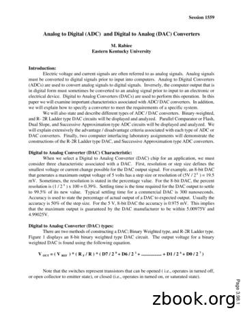
What is a Digital Analog Converter? Introduction In electronics, a digital-to-analog converter (DAC or D-to-A) is a device for converting a digital (usually binary) code to an analog signal (current, voltage or electric charge). An analog-to-digital converter (ADC) performs the
Figure 6. Three-bit, Flash Type Analog to Digital Converter Circuit Analog to Digital Converter (ADC): When selecting an Analog to Digital converter (ADC) chip for an application, three characteristics must be considered. Similar t
II. Evolution of the Analog RF-Digital Interface The analog RF-digital interface is significantly affected by the placement of the analog-to-digital converter (ADC)/digital-to-analog converter (DAC) pair. For most of the wireless systems designed in the 1990s, the ADC/ DACs we
A DSP System A/D DSP D/A Analog signal Analog signal Sampled data signal Analog signal Cts-time dst-amp staricase signal Digital signal Digital signal DSP System Antialiasing Filter Sample and Hold Reconstruction Filter A/D: Iconverts a sampled data signal value into a digital number, in part, through quantization of the amplitude


